- 您现在的位置:买卖IC网 > PDF目录1939 > MAX3386EEUP (Maxim Integrated Products)IC TXRX RS232 250KBPS 20-TSSOP PDF资料下载
参数资料
| 型号: | MAX3386EEUP |
| 厂商: | Maxim Integrated Products |
| 文件页数: | 4/11页 |
| 文件大小: | 0K |
| 描述: | IC TXRX RS232 250KBPS 20-TSSOP |
| 产品培训模块: | Lead (SnPb) Finish for COTS Obsolescence Mitigation Program |
| 标准包装: | 74 |
| 类型: | 收发器 |
| 驱动器/接收器数: | 3/2 |
| 规程: | RS232 |
| 电源电压: | 3 V ~ 5.5 V |
| 安装类型: | 表面贴装 |
| 封装/外壳: | 20-TSSOP(0.173",4.40mm 宽) |
| 供应商设备封装: | 20-TSSOP |
| 包装: | 管件 |
IOUT = -1mA
MAX3386E
3.0V, ±25kV ESD-Protected RS-232
Transceiver for PDAs and Cell Phones
2
_______________________________________________________________________________________
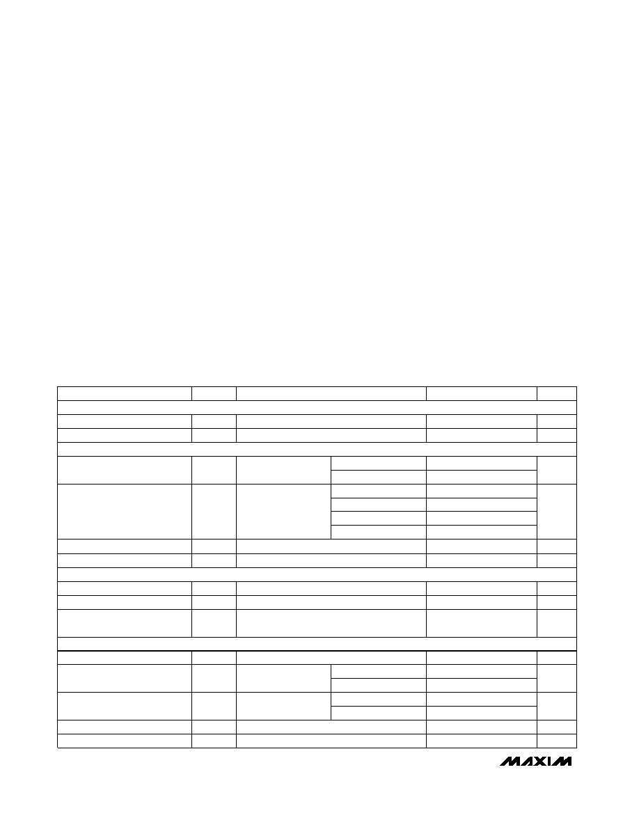
ABSOLUTE MAXIMUM RATINGS
DC ELECTRICAL CHARACTERISTICS
(VCC = VL = +3.0V to +5.5V; C1–C4 = 0.1F, tested at +3.3V ±10%; C1 = 0.047F, C2–C4 = 0.33F, tested at +5.0V ±10%; TA =
TMIN to TMAX; unless otherwise noted. Typical values are at VCC = VL = +3.3V, TA = +25°C.)
Stresses beyond those listed under “Absolute Maximum Ratings” may cause permanent damage to the device. These are stress ratings only, and functional
operation of the device at these or any other conditions beyond those indicated in the operational sections of the specifications is not implied. Exposure to
absolute maximum rating conditions for extended periods may affect device reliability.
Note 1: V+ and V- can have maximum magnitudes of 7V, but their absolute difference cannot exceed 13V.
VCC to GND ..............................................................-0.3V to +6V
VL to GND...................................................-0.3V to (VCC + 0.3V)
V+ to GND ................................................................-0.3V to +7V
V- to GND .................................................................+0.3V to -7V
V+ +
V-(Note 1) .............................................................. +13V
Input Voltages
T_IN, SHDN to GND ...........................................-0.3V to +6V
R_IN to GND ..................................................................±25V
Output Voltages
T_OUT to GND............................................................±13.2V
R_OUT.....................................................-0.3V to (VL + 0.3V)
Short-Circuit Duration T_OUT to GND........................Continuous
Continuous Power Dissipation (TA = +70°C)
20-Pin TSSOP (derate 7.0mW/°C above +70°C) .......559mW
Operating Temperature Ranges
MAX3386ECUP .................................................0°C to +70°C
MAX3386EEUP ..............................................-40°C to +85°C
Junction Temperature ......................................................+150°C
Storage Temperature Range .............................-65°C to +150°C
Lead Temperature (soldering, 10s) .................................+300°C
IOUT = 1.6mA
R_OUT, receivers disabled
T_IN, SHDN
SHDN = GND, all inputs at VCC or GND
SHDN = VCC, no load
CONDITIONS
V
0.4
Output Voltage Low
A
±0.05
±10
Output Leakage Currents
A
±0.01
±1
Input Leakage Current
V
0.5
Transmitter Input Hysteresis
V
0.9
Input Logic Threshold High
1.4
2.0
2.4
V
0.8
110
A
Shutdown Supply Current
mA
0.3
1
Supply Current
UNITS
MIN
TYP
MAX
SYMBOL
PARAMETER
VL = 5.0V
VL = 3.3V
VL = 2.5V
VL = 1.8V
IOUT = -1mA
V
VL -
0.6
0.1
Output Voltage High
VL = 3.3V or 5.0V
T_IN, SHDN
0.6
Input Logic Threshold Low
VL = 2.5V
V
-25
+25
Input Voltage Range
TA = +25°C
V
0.8
1.2
Input Threshold Low
0.6
1.5
VL = 5.0V
VL = 3.3V
TA = +25°C
V
1.8
2.4
Input Threshold High
1.5
2.4
VL = 5.0V
VL = 3.3V
V
0.5
Input Hysteresis
35
7
TA = +25°C
k
Input Resistance
DC CHARACTERISTICS (VCC = +3.3V or +5V, TA = +25°C)
LOGIC INPUTS
RECEIVER OUTPUTS
RECEIVER INPUTS
相关PDF资料 |
PDF描述 |
|---|---|
| MAX3387EEUG | IC TXRX RS232 250KBPS 24-TSSOP |
| MAX3388ECUG | IC TXRX RS232 250KBPS 24-TSSOP |
| MAX339ESE | IC MULTIPLEXER DUAL 4X1 16SOIC |
| MAX3408EUK+T | IC TERMINATION NETWORK SOT23-5 |
| MAX3420EECJ+T | IC USB PERIPH CONTROLLER 32TQFP |
相关代理商/技术参数 |
参数描述 |
|---|---|
| MAX3386EEUP+ | 功能描述:RS-232接口集成电路 3V Transceiver for PDAs & Cells RoHS:否 制造商:Exar 数据速率:52 Mbps 工作电源电压:5 V 电源电流:300 mA 工作温度范围:- 40 C to + 85 C 安装风格:SMD/SMT 封装 / 箱体:LQFP-100 封装: |
| MAX3386EEUP+T | 功能描述:RS-232接口集成电路 3V Transceiver for PDAs & Cells RoHS:否 制造商:Exar 数据速率:52 Mbps 工作电源电压:5 V 电源电流:300 mA 工作温度范围:- 40 C to + 85 C 安装风格:SMD/SMT 封装 / 箱体:LQFP-100 封装: |
| MAX3386EEUP-T | 功能描述:RS-232接口集成电路 RoHS:否 制造商:Exar 数据速率:52 Mbps 工作电源电压:5 V 电源电流:300 mA 工作温度范围:- 40 C to + 85 C 安装风格:SMD/SMT 封装 / 箱体:LQFP-100 封装: |
| MAX3386EIDW | 功能描述:RS-232接口集成电路 RS-232 Line Driver/Receiver RoHS:否 制造商:Exar 数据速率:52 Mbps 工作电源电压:5 V 电源电流:300 mA 工作温度范围:- 40 C to + 85 C 安装风格:SMD/SMT 封装 / 箱体:LQFP-100 封装: |
| MAX3386EIDWG4 | 功能描述:RS-232接口集成电路 RS-232 Line Driver/Receiver RoHS:否 制造商:Exar 数据速率:52 Mbps 工作电源电压:5 V 电源电流:300 mA 工作温度范围:- 40 C to + 85 C 安装风格:SMD/SMT 封装 / 箱体:LQFP-100 封装: |
发布紧急采购,3分钟左右您将得到回复。