- 您现在的位置:买卖IC网 > PDF目录8846 > MAX3393EEUD+T (Maxim Integrated Products)IC LVL XLTR LV 8MBPS 14-TSSOP PDF资料下载
参数资料
| 型号: | MAX3393EEUD+T |
| 厂商: | Maxim Integrated Products |
| 文件页数: | 3/26页 |
| 文件大小: | 0K |
| 描述: | IC LVL XLTR LV 8MBPS 14-TSSOP |
| 产品培训模块: | Lead (SnPb) Finish for COTS Obsolescence Mitigation Program |
| 标准包装: | 2,500 |
| 逻辑功能: | 变换器,单向,3 态,开路漏极 |
| 位数: | 4 |
| 输入类型: | 逻辑 |
| 输出类型: | 逻辑 |
| 数据速率: | 16Mbps |
| 通道数: | 4 |
| 输出/通道数目: | 1 |
| 差分 - 输入:输出: | 无/无 |
| 传输延迟(最大): | 15ns |
| 电源电压: | 1.65 V ~ 5.5 V |
| 工作温度: | -40°C ~ 85°C |
| 封装/外壳: | 14-TSSOP(0.173",4.40mm 宽) |
| 供应商设备封装: | 14-TSSOP |
| 包装: | 带卷 (TR) |
MAX3372E–MAX3379E/MAX3390E–MAX3393E
±15kV ESD-Protected, 1A, 16Mbps, Dual/Quad
Low-Voltage Level Translators in UCSP
11
Maxim Integrated
Level Translation
For proper operation ensure that +1.65V
≤ VCC ≤
+5.5V, +1.2V
≤ VL ≤ +5.5V, and VL ≤ (VCC + 0.3V).
During power-up sequencing, VL
≥ (VCC + 0.3V) will
not damage the device. During power-supply sequenc-
ing, when VCC is floating and VL is powering up, a cur-
rent may be sourced, yet the device will not latch up.
The speed-up circuitry limits the maximum data rate for
devices in the MAX3372E–MAX3379E, MAX3390E–
MAX3393E family to 16Mbps. The maximum data rate
also depends heavily on the load capacitance (see the
Typical Operating Characteristics), output impedance
of the driver, and the operational voltage range (see the
Timing Characteristics table).
Speed-Up Circuitry
The MAX3373E–MAX3376E/MAX3378E/MAX3379E and
MAX3390E–MAX3393E feature a one-shot generator that
decreases the rise time of the output. When triggered,
MOSFETs PU1 and PU2 turn on for a short time to pull up
I/O VL_ and I/O VCC_ to their respective supplies (see
Figure 2b). This greatly reduces the rise time and propa-
gation delay for the low-to-high transition. The scope
photo of Rail-to-Rail Driving for 8Mbps Operation in the
Typical Operating Characteristics shows the speed-up
circuitry in operation.
Rise-Time Accelerators
The MAX3373E–MAX3376E/MAX3378E/MAX3379E and
the MAX3390E–MAX3393E have internal rise-time
accelerators allowing operation up to 16Mbps. The
rise-time accelerators are present on both sides of the
device and act to speed up the rise time of the input
and output of the device, regardless of the direction of
the data. The triggering mechanism for these accelera-
tors is both level and edge sensitive. To prevent false
triggering of the rise-time accelerators, signal fall times
of less than 20ns/V are recommended for both the
inputs and outputs of the device. Under less noisy con-
ditions, longer signal fall times may be acceptable.
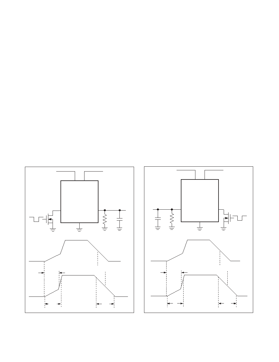
MAX3372E–MAX3379E
AND MAX3390E–MAX3393E
I/O VL_
I/O VCC_
VCC
VL
GND
I/O VCC_
tPD-VCC-LH
tPD-VCC-HL
I/O VL_
tRVCC
tFVCC
DATA
RLOAD
CLOAD
Figure 1c. Open-Drain Driving I/O VCC
MAX3373E–MAX3376E,
MAX3378E/MAX3379E
AND MAX3390E–MAX3393E
I/O VL_
I/O VCC_
DATA
I/O VCC_
VCC
VL
GND
RLOAD
CLOAD
tPD-VL-LH
tPD-VL-HL
I/O VL_
tRVL
tFVL
Figure 1d. Open-Drain Driving I/O VL
相关PDF资料 |
PDF描述 |
|---|---|
| MAX3392EEUD+T | IC LVL XLTR LV 8MBPS 14-TSSOP |
| D38999/24WD5AC | CONN HSG RCPT 5POS JAM NUT PINS |
| MS27467T21B39A | CONN HSG PLUG 39POS STRGHT PINS |
| V28B5M75BG2 | CONVERTER MOD DC/DC 5V 75W |
| VE-B2L-MY-F1 | CONVERTER MOD DC/DC 28V 50W |
相关代理商/技术参数 |
参数描述 |
|---|---|
| MAX3394EEBL | 制造商:Maxim Integrated Products 功能描述:+/-15KV ESD-PROTECT HI DRIVE CURR - Rail/Tube |
| MAX3394EEBL+ | 制造商:Maxim Integrated Products 功能描述:15KV ESD-PROTECTED, HIGH-DRIVE CURRENT, DUAL-/QUAD- - Rail/Tube |
| MAX3394EEBL+T | 功能描述:转换 - 电压电平 High-Drive Current RoHS:否 制造商:Micrel 类型:CML/LVDS/LVPECL to LVCMOS/LVTTL 传播延迟时间:1.9 ns 电源电流:14 mA 电源电压-最大:3.6 V 电源电压-最小:3 V 最大工作温度:+ 85 C 安装风格:SMD/SMT 封装 / 箱体:MLF-8 |
| MAX3394EEBL+TG45 | 功能描述:转换 - 电压电平 High-Drive Current RoHS:否 制造商:Micrel 类型:CML/LVDS/LVPECL to LVCMOS/LVTTL 传播延迟时间:1.9 ns 电源电流:14 mA 电源电压-最大:3.6 V 电源电压-最小:3 V 最大工作温度:+ 85 C 安装风格:SMD/SMT 封装 / 箱体:MLF-8 |
| MAX3394EEBL-T | 功能描述:转换 - 电压电平 RoHS:否 制造商:Micrel 类型:CML/LVDS/LVPECL to LVCMOS/LVTTL 传播延迟时间:1.9 ns 电源电流:14 mA 电源电压-最大:3.6 V 电源电压-最小:3 V 最大工作温度:+ 85 C 安装风格:SMD/SMT 封装 / 箱体:MLF-8 |
发布紧急采购,3分钟左右您将得到回复。