- 您现在的位置:买卖IC网 > PDF目录11587 > MAX3420EETG+ (Maxim Integrated Products)IC USB PERIPH CONTROLLER 24TQFN PDF资料下载
参数资料
| 型号: | MAX3420EETG+ |
| 厂商: | Maxim Integrated Products |
| 文件页数: | 6/22页 |
| 文件大小: | 0K |
| 描述: | IC USB PERIPH CONTROLLER 24TQFN |
| 产品培训模块: | Lead (SnPb) Finish for COTS Obsolescence Mitigation Program |
| 标准包装: | 75 |
| 控制器类型: | USB 外设控制器 |
| 接口: | USB/串行 |
| 电源电压: | 3 V ~ 3.6 V |
| 电流 - 电源: | 15mA |
| 工作温度: | -40°C ~ 85°C |
| 安装类型: | 表面贴装 |
| 封装/外壳: | 24-WFQFN 裸露焊盘 |
| 供应商设备封装: | 24-TQFN-EP(4x4) |
| 包装: | 管件 |
| 产品目录页面: | 1407 (CN2011-ZH PDF) |
| 配用: | MAX3420EEVKIT-2+-ND - EVAL KIT FOR MAX3420E |
pending (Figure 10). Set the POSINT bit in the PINCTL
(R17) register to make INT active high, and clear the
POSINT bit to make INT active low.
GPIN3–GPIN0, GPOUT3–GPOUT0 and GPX
The MAX3420E has four general-purpose inputs
(GPIN3–GPIN0), four general-purpose outputs
(GPOUT3–GPOUT0), and a multiplexed output pin
(GPX). GPIN3 through GPIN0 all have weak internal
pullup resistors to VL. These inputs can be read by
sampling bits 7 through 4 of the IOPINS (R20) register.
Writing to GPIN3 through GPIN0 has no effect.
GPOUT3 through GPOUT0 are the general-purpose
outputs. Update these outputs by writing to bits 3
through 0 of the IOPINS (R20) register. GPOUT3–
GPOUT0 logic levels are referenced to the voltage on
VL. As shown in Figure 11, reading the state of a
GPOUT3–GPOUT0 bit returns the state of the internal
register bit, not the actual pin state. This is useful for
doing read-modify-write operations to an output pin
(such as blinking an LED), since the load on the output
pin does not affect the register logic state.
GPX is a push-pull output with a 4-way multiplexer that
selects its output signal. The logic level on GPX is refer-
enced to VL. The SPI master writes to the GPXB and
GPXA bits of PINCTL (R17) register to select one of four
internal signals as depicted in Table 3.
OPERATE: This signal goes high when the
MAX3420E is able to operate after a power-up or
RES reset. OPERATE is the default GPX output.
VBUS_DET: VBUS_DET is the VBCOMP comparator
output. This allows the user to directly monitor the
VBUS status.
BUSACT: USB BUS activity signal (active-high).
This signal is active whenever there is traffic on
the USB bus. The BUSACT signal is set whenever
a SYNC field is detected. BUSACT goes low during
bus reset or after 32-bit times of J-state.
SOF: A square wave with a positive edge that
indicates the USB start-of-frame (Figure 12).
MOSI (Master-Out, Slave-In) and
MISO (Master-In, Slave-Out)
The SPI data pins MOSI and MISO operate differently
depending on the setting of a register bit called FDUPSPI
(full-duplex SPI). Figure 13 shows the two configurations
according to the FDUPSPI bit setting.
USB Peripheral Controller
with SPI Interface
REGISTER BIT
GPOUT
WRITE
GPOUT
READ
GPOUT
PIN
Figure 11. Behavior of Read and Write Operations on
GPOUT3–GPOUT0
Table 3. GPX Output State
GPXB
GPXA
GPX PIN OUTPUT
0
OPERATE (Default State)
0
1
VBUS_DET
1
0
BUSACT
1
SOF
FULL-SPEED
TIME FRAME
1ms
FULL-SPEED
TIME FRAME
1ms
SOF
USB
PACKETS
GPX
SOF
~50%
Figure 12. GPX Output in SOF Mode
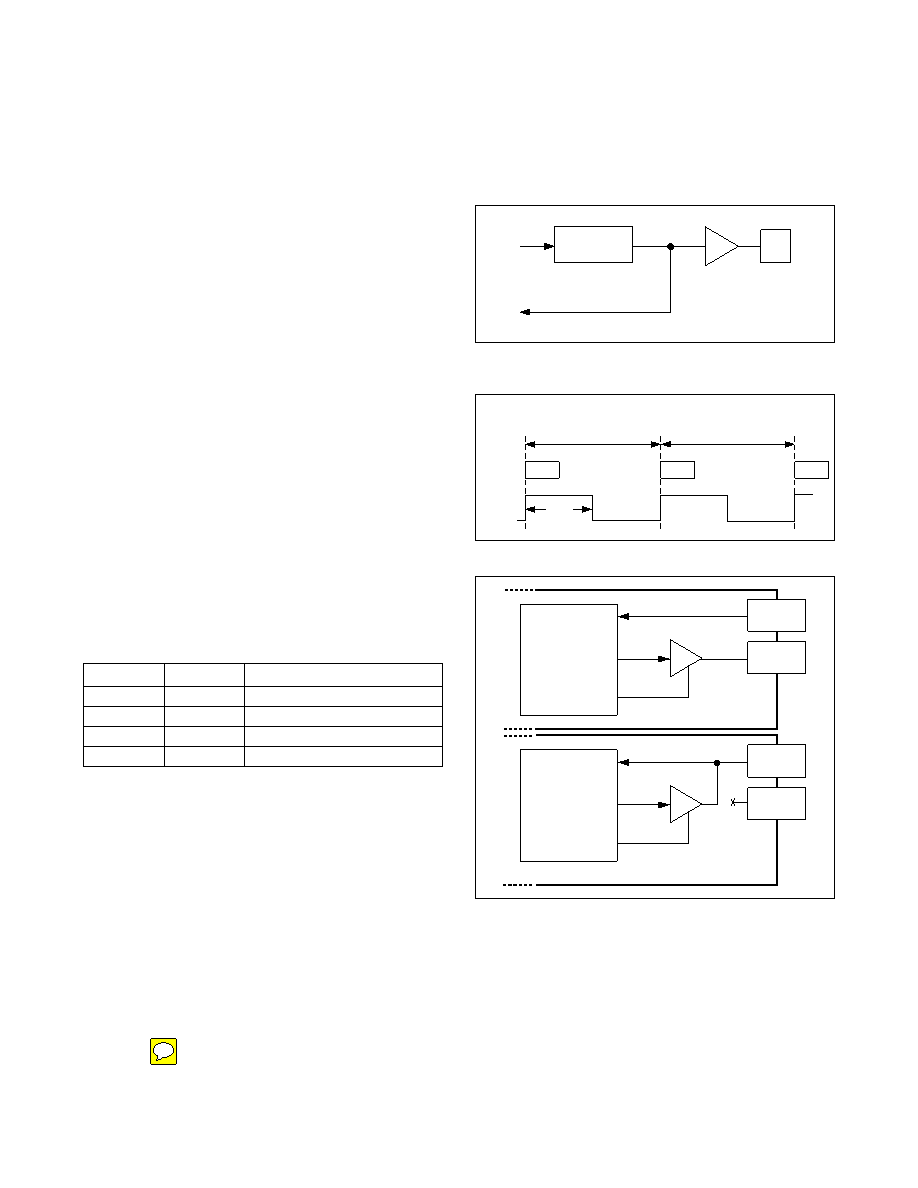
FDUPSPI = 1
FDUPSPI = 0
(DEFAULT)
MAX3420E
MOSI
MISO
MOSI
MISO
Figure 13. MAX3420E SPI Data Pins for Full-Duplex (Top) and
Half-Duplex (Bottom) Operation
MAX3420E
14
Maxim Integrated
相关PDF资料 |
PDF描述 |
|---|---|
| PIC12F629-E/SN | IC MCU CMOS 8BIT 1K FLASH 8-SOIC |
| PIC12LC508A-04I/MF | IC MCU OTP 512X12 LV 8DFN |
| PIC16F631-E/P | IC PIC MCU FLASH 1KX14 20DIP |
| PIC16C620A-04I/SO | IC MCU OTP 512X14 COMP 18SOIC |
| PIC12CE518-04I/SN | IC MCU OTP 512X12 W/EE 8SOIC |
相关代理商/技术参数 |
参数描述 |
|---|---|
| MAX3420EETG+ | 功能描述:外围驱动器与原件 - PCI USB Peripheral Controller w/SPI RoHS:否 制造商:PLX Technology 工作电源电压: 最大工作温度: 安装风格:SMD/SMT 封装 / 箱体:FCBGA-1156 封装:Tray |
| MAX3420EETG+T | 功能描述:外围驱动器与原件 - PCI USB Peripheral Controller w/SPI RoHS:否 制造商:PLX Technology 工作电源电压: 最大工作温度: 安装风格:SMD/SMT 封装 / 箱体:FCBGA-1156 封装:Tray |
| MAX3420EETG-T | 功能描述:外围驱动器与原件 - PCI RoHS:否 制造商:PLX Technology 工作电源电压: 最大工作温度: 安装风格:SMD/SMT 封装 / 箱体:FCBGA-1156 封装:Tray |
| MAX3420EEVKIT | 制造商:Maxim Integrated Products 功能描述:MAX3420E EVAL KIT - Bulk |
| MAX3420EEVKIT-2+ | 功能描述:界面开发工具 MAX3420E Eval Kit RoHS:否 制造商:Bourns 产品:Evaluation Boards 类型:RS-485 工具用于评估:ADM3485E 接口类型:RS-485 工作电源电压:3.3 V |
发布紧急采购,3分钟左右您将得到回复。