- 您现在的位置:买卖IC网 > PDF目录10501 > MAX3430CPA+ (Maxim Integrated Products)IC TXRX RS-485 3.3V 8-DIP PDF资料下载
参数资料
| 型号: | MAX3430CPA+ |
| 厂商: | Maxim Integrated Products |
| 文件页数: | 2/13页 |
| 文件大小: | 0K |
| 描述: | IC TXRX RS-485 3.3V 8-DIP |
| 产品培训模块: | Lead (SnPb) Finish for COTS Obsolescence Mitigation Program |
| 标准包装: | 50 |
| 类型: | 收发器 |
| 驱动器/接收器数: | 1/1 |
| 规程: | RS485 |
| 电源电压: | 3 V ~ 3.6 V |
| 安装类型: | 通孔 |
| 封装/外壳: | 8-DIP(0.300",7.62mm) |
| 供应商设备封装: | 8-PDIP |
| 包装: | 管件 |
| 产品目录页面: | 1407 (CN2011-ZH PDF) |
MAX3430
±80V Fault-Protected, Fail-Safe,
1/4-Unit Load, +3.3V RS-485 Transceiver
10
______________________________________________________________________________________
stage, provides immediate protection against short cir-
cuits over the whole common-mode voltage range. The
second, a thermal shutdown circuit, forces the driver
outputs into a high-impedance state if the die tempera-
ture exceeds +160°C. Normal operation resumes when
the die temperature cools by +140°C, resulting in a
pulsed output during continuous short-circuit conditions.
Hot-Swap Capability
Hot-Swap Inputs
Inserting circuit boards into a hot, or powered backplane
may cause voltage transients on DE, RE, and receiver
inputs A and B that can lead to data errors. For example,
upon initial circuit board insertion, the processor under-
goes a power-up sequence. During this period, the high-
impedance state of the output drivers makes them
unable to drive the MAX3430 enable inputs to a defined
logic level. Meanwhile, leakage currents of up to 10A
from the high-impedance output, or capacitively coupled
noise from VCC or GND, could cause an input to drift to
an incorrect logic state. To prevent such a condition from
occurring, the MAX3430 features hot-swap input circuitry
on DE to safeguard against unwanted driver activation
during hot-swap situations. When VCC rises, an internal
pulldown circuit holds DE low for at least 10s, and until
the current into DE exceeds 200A. After the initial
power-up sequence, the pulldown circuit becomes
transparent, resetting the hot-swap tolerable input.
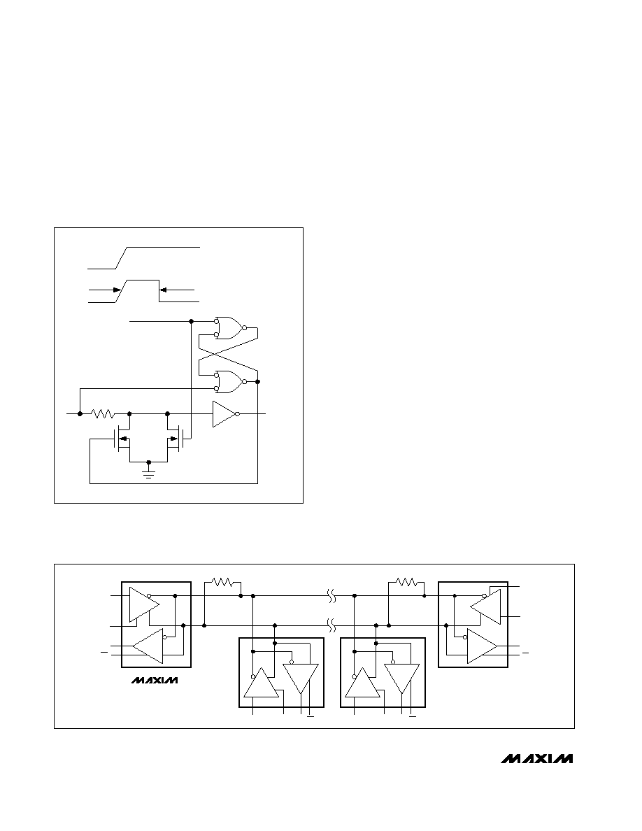
Hot-Swap Input Circuitry
At the driver enable input (DE), there are two NMOS
devices, M1 and M2 (Figure 9). When VCC ramps from
0, an internal 15s timer turns on M2 and sets the SR
latch, which also turns on M1. Transistors M2, a 2mA
current sink, and M1, a 100A current sink, pull DE to
GND through a 5.6k
resistor. M2 pulls DE to the dis-
abled state against an external parasitic capacitance
up to 100pF that may drive DE high. After 15s, the
timer deactivates M2 while M1 remains on, holding DE
low against three-state leakage currents that may drive
DE high. M1 remains on until an external current source
overcomes the required input current. At this time, the
SR latch resets M1 and turns off. When M1 turns off, DE
reverts to a standard, high-impedance CMOS input.
Whenever VCC drops below 1V, the input is reset.
VCC
TIMER
DE
(HOT SWAP)
15
s
100
A
M1
M2
5.6k
2mA
Figure 9. Simplified Structure of the Driver Enable Pin (DE)
DI
RO
DE
A
B
RE
RO
DI
DE
RE
DE
D
R
BB
B
A
120
120
D
R
MAX3430
RE
Figure 10. Typical RS-485 Network
相关PDF资料 |
PDF描述 |
|---|---|
| MAX243CWE+ | IC RS-232 DRVR/RCVR 16-SOIC |
| MAX11212BEUB+ | IC ADC 18BIT SRL 13.75SPS 10UMAX |
| MAX11619EEE+ | IC ADC 10BIT SRL 300KSPS 16QSOP |
| VI-B4F-MW | CONVERTER MOD DC/DC 72V 100W |
| MAX11618EEE+ | IC ADC 10BIT SRL 300KSPS 16QSOP |
相关代理商/技术参数 |
参数描述 |
|---|---|
| MAX3430CPA+ | 功能描述:RS-485接口IC Fail-Safe 1/4-Unit 3.3V Transceiver RoHS:否 制造商:Texas Instruments 数据速率:250 Kbps 工作电源电压:3.3 V 电源电流:750 uA 工作温度范围:- 40 C to + 125 C 安装风格:SMD/SMT 封装 / 箱体:SOIC-8 封装:Tube |
| MAX3430CSA | 功能描述:RS-485接口IC RoHS:否 制造商:Texas Instruments 数据速率:250 Kbps 工作电源电压:3.3 V 电源电流:750 uA 工作温度范围:- 40 C to + 125 C 安装风格:SMD/SMT 封装 / 箱体:SOIC-8 封装:Tube |
| MAX3430CSA+ | 功能描述:RS-485接口IC Fail-Safe 1/4-Unit 3.3V Transceiver RoHS:否 制造商:Texas Instruments 数据速率:250 Kbps 工作电源电压:3.3 V 电源电流:750 uA 工作温度范围:- 40 C to + 125 C 安装风格:SMD/SMT 封装 / 箱体:SOIC-8 封装:Tube |
| MAX3430CSA+T | 功能描述:RS-485接口IC Fail-Safe 1/4-Unit 3.3V Transceiver RoHS:否 制造商:Texas Instruments 数据速率:250 Kbps 工作电源电压:3.3 V 电源电流:750 uA 工作温度范围:- 40 C to + 125 C 安装风格:SMD/SMT 封装 / 箱体:SOIC-8 封装:Tube |
| MAX3430CSA-T | 功能描述:RS-485接口IC RoHS:否 制造商:Texas Instruments 数据速率:250 Kbps 工作电源电压:3.3 V 电源电流:750 uA 工作温度范围:- 40 C to + 125 C 安装风格:SMD/SMT 封装 / 箱体:SOIC-8 封装:Tube |
发布紧急采购,3分钟左右您将得到回复。