- 您现在的位置:买卖IC网 > PDF目录385526 > MAX3451E (Maxim Integrated Products, Inc.) ?5kV ESD-Protected USB Transceivers PDF资料下载
参数资料
| 型号: | MAX3451E |
| 厂商: | Maxim Integrated Products, Inc. |
| 英文描述: | ?5kV ESD-Protected USB Transceivers |
| 中文描述: | 具有±15kV ESD保护的USB收发器 |
| 文件页数: | 2/16页 |
| 文件大小: | 379K |
| 代理商: | MAX3451E |
M
±15kV ESD-Protected USB Transceivers
2
_______________________________________________________________________________________
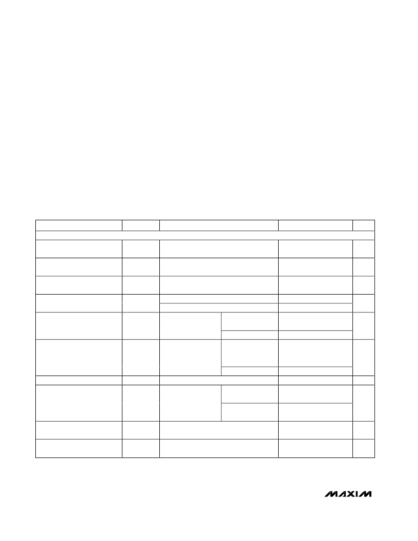
ABSOLUTE MAXIMUM RATINGS
V
BUS
, V
L
, D+, D- to GND.......................................-0.3V to +6.0V
V
TRM
to GND ............................................-0.3V to (V
BUS
+ 0.3V)
VP, VM, SUS, SPD, ENUM,
RCV,
OE
, BD to GND................................-0.3V to (V
L
+ 0.3V)
Current (into any pin)........................................................
±
15mA
Short-Circuit Current (D+ and D-)...................................
±
150mA
Stresses beyond those listed under “Absolute Maximum Ratings” may cause permanent damage to the device. These are stress ratings only, and functional
operation of the device at these or any other conditions beyond those indicated in the operational sections of the specifications is not implied. Exposure to
absolute maximum rating conditions for extended periods may affect device reliability.
DC ELECTRICAL CHARACTERISTICS
(V
BUS
= +4.0V to +5.5V or V
TRM
= +3.0V to +3.6V, V
L
= +1.65V to +3.6V, T
A
= T
MIN
to T
MAX
, unless otherwise noted. Typical values
are at V
BUS
= +5.0V, V
L
= +2.5V, and T
A
= +25
°
C.) (Note 1)
PARAMETER
SYM B O L
CONDITIONS
MIN
TYP
MAX
UNITS
SUPPLY INPUTS (V
BUS
, V
TRM
, V
L
)
Regulated Supply Voltage
Output
V
TRM
Internal regulator
3.0
3.3
3.6
V
Operating Supply Current
I
VBUS
Full-speed transmitting/receiving at 12Mbps,
C
L
= 50pF on D+ and D- (Note 2)
10
mA
Operating V
L
Supply Current
I
VL
Full-speed transmitting/receiving at 12Mbps
(Note 2)
2.5
mA
Full-speed idle: V
D+
> 2.7V, V
D-
< 0.3V
SE0: V
D+
< 0.3V, V
D-
< 0.3V
250
250
350
350
Full-Speed Idle and SE0 Supply
Current
I
VBUS(IDLE)
μA
MAX3450E,
MAX3451E
5
Static V
L
Supply Current
I
VL(STATIC)
Full-speed idle,
SE0, or suspend
mode
MAX3452E
15
μA
MAX3450E,
MAX3451E
(ENUM = low)
35
Suspend Supply Current
I
VBUS(SUSP)
VM = VP = open,
SUS =
OE
= high
MAX3452E
40
20
μA
Disable-Mode Supply Current
I
VBUS(DIS)
V
L
= GND or open
μA
MAX3450E,
MAX3451E
5
Sharing-Mode V
L
Supply
Current
I
VL(SHARING)
V
BUS
= GND or open,
OE
= low, VP = low or
high, VM = low or
high, SUS = high
MAX3452E
20
μA
D+/D- Sharing-Mode
Load Current
I
D_(SHARING)
V
BUS
= GND or open, V
D_
= 0 or +5.5V
20
μA
D+/D- Disable-Mode
Load Current
I
D_(DIS)
V
L
= GND or open, V
D_
= 0 or +5.5V
5
μA
Continuous Power Dissipation (T
A
= +70
°
C)
14-Pin TSSOP
(derate 9.1mW/
°
C above +70
°
C).................................727mW
16-Pin Thin QFN 3mm x 3mm
(derate 14.7mW/
°
C above +70
°
C).............................1176mW
Operating Temperature Range ...........................-40
°
C to +85
°
C
Junction Temperature......................................................+150
°
C
Storage Temperature Range.............................-65
°
C to +150
°
C
Lead Temperature (soldering, 10s).................................+300
°
C
相关PDF资料 |
PDF描述 |
|---|---|
| MAX3452E | ?5kV ESD-Protected USB Transceivers |
| MAX3450EEUD | 【15kV ESD-Protected USB Transceivers |
| MAX3451EEUD | 【15kV ESD-Protected USB Transceivers |
| MAX3452EEUD | 【15kV ESD-Protected USB Transceivers |
| MAX3450EETE | Single Full-Duplex LVDS Transceiver 14-SOIC -40 to 85 |
相关代理商/技术参数 |
参数描述 |
|---|---|
| MAX3451EETE | 功能描述:USB 接口集成电路 RoHS:否 制造商:Cypress Semiconductor 产品:USB 2.0 数据速率: 接口类型:SPI 工作电源电压:3.15 V to 3.45 V 工作电源电流: 最大工作温度:+ 85 C 安装风格:SMD/SMT 封装 / 箱体:WLCSP-20 |
| MAX3451EETE-T | 功能描述:USB 接口集成电路 RoHS:否 制造商:Cypress Semiconductor 产品:USB 2.0 数据速率: 接口类型:SPI 工作电源电压:3.15 V to 3.45 V 工作电源电流: 最大工作温度:+ 85 C 安装风格:SMD/SMT 封装 / 箱体:WLCSP-20 |
| MAX3451EEUD | 功能描述:USB 接口集成电路 RoHS:否 制造商:Cypress Semiconductor 产品:USB 2.0 数据速率: 接口类型:SPI 工作电源电压:3.15 V to 3.45 V 工作电源电流: 最大工作温度:+ 85 C 安装风格:SMD/SMT 封装 / 箱体:WLCSP-20 |
| MAX3451EEUD+ | 功能描述:USB 接口集成电路 USB Transceiver RoHS:否 制造商:Cypress Semiconductor 产品:USB 2.0 数据速率: 接口类型:SPI 工作电源电压:3.15 V to 3.45 V 工作电源电流: 最大工作温度:+ 85 C 安装风格:SMD/SMT 封装 / 箱体:WLCSP-20 |
| MAX3451EEUD+T | 功能描述:USB 接口集成电路 USB Transceiver RoHS:否 制造商:Cypress Semiconductor 产品:USB 2.0 数据速率: 接口类型:SPI 工作电源电压:3.15 V to 3.45 V 工作电源电流: 最大工作温度:+ 85 C 安装风格:SMD/SMT 封装 / 箱体:WLCSP-20 |
发布紧急采购,3分钟左右您将得到回复。