参数资料
| 型号: | MAX34565EVKIT# |
| 厂商: | Maxim Integrated Products |
| 文件页数: | 8/10页 |
| 文件大小: | 0K |
| 描述: | KIT EVAL FOR MAX34565 |
| 产品培训模块: | Obsolescence Mitigation Program |
| 标准包装: | 1 |
| 系列: | * |
�� �
�
�MAX34565�
�12V� Hot-Plug� Switch� in� TDFN� Package�
�Latchoff� Version�
�Once� the� latchoff� version� has� entered� thermal� shutdown,�
�it� does� not� attempt� to� turn� back� on.� The� only� way� to� turn�
�this� device� back� on� is� to� cycle� the� power� to� the� device.�
�When� power� is� reapplied� ton� the� V� CC� pad,� the� junction�
�temperature� needs� to� be� less� than� T� SHDN� for� the� device�
�to� be� enabled.�
�Applications� Information�
�Exposed� Pad� (V� CC� )�
�The� exposed� pad� is� the� voltage� supply� pin� for� the� device�
�and� should� be� connected� to� a� large� trace� or� plane.� The�
�exposed� pad� also� acts� as� a� heatsink,� and� can� dissipate�
�heat� from� the� device.�
�R� ILIM� .� To� greatly� reduce� this� offset,� it� is� recommended�
�that� one� of� the� LOAD� pins� have� a� dedicated� connection�
�to� ILIM� though� R� ILIM� ,� and� not� be� used� to� pass� the� LOAD�
�current,� I� LOAD� (� Figure� 6� ).� This� would� leave� four� LOAD�
�pins� to� pass� I� LOAD� ,� which� should� be� sufficient.� Because�
�there� is� only� a� small� amount� of� current� passed� from� this�
�lone� LOAD� pin� to� ILIM,� there� is� a� negligible� voltage� offset�
�applied� to� the� internal� comparator.� This� method� is� the�
�best� way� to� attain� an� accurate� current� limit� for� I� LOAD� .�
�V� CC�
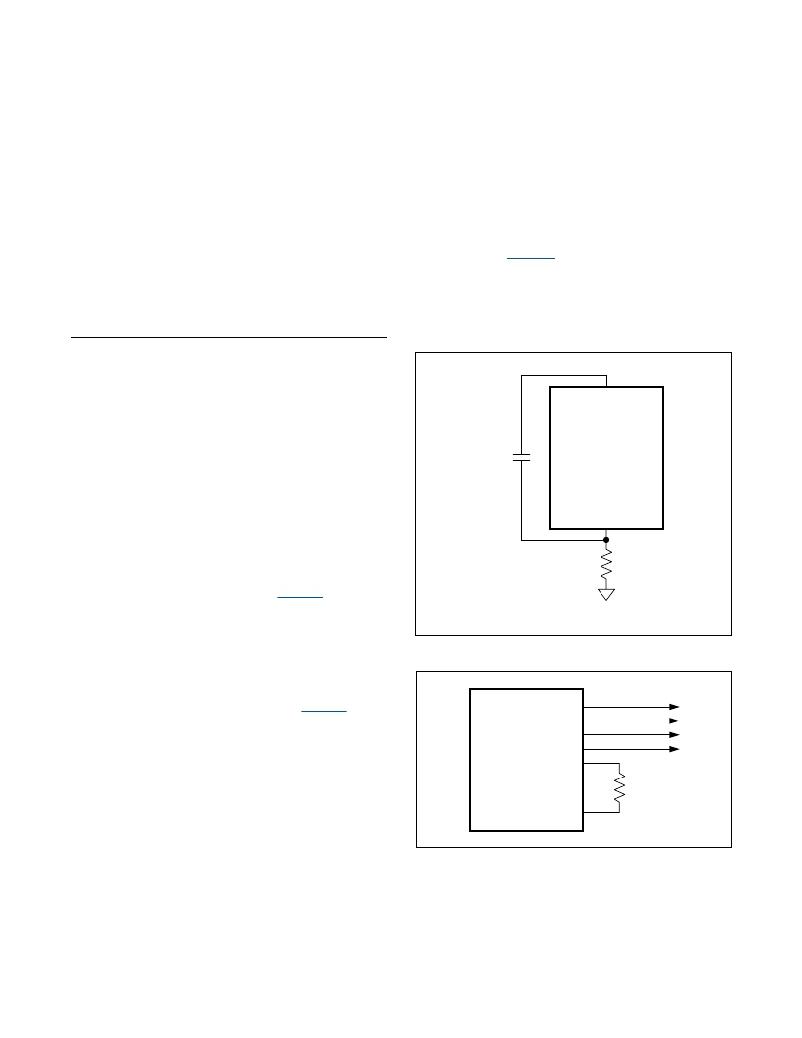
�Decoupling� Capacitors�
�It� is� of� utmost� importance� to� properly� bypass� the� device’s�
�supply� pins.� A� decoupling� capacitor� absorbs� the� energy�
�stored� in� the� supply� and� board� parasitic� inductance� when�
�the� FET� is� turned� off,� thereby� reducing� the� magnitude� of�
�overshoot� of� V� CC� .� This� can� be� accomplished� by� using� a�
�high-quality� (low� ESR,� low� ESL)� ceramic� capacitor� sol-�
�dered� directly� between� the� V� CC� and� GND� connections.�
�Any� series� resistance� with� this� bypass� capacitor� lowers�
�its� effectiveness� and� is� not� recommended.� A� minimum�
�0.5� F� F� ceramic� capacitor� is� required� (� Figure� 5� ).� However,�
�0.5μF�
�MINIMUM�
�REQUIRED�
�MAX34565�
�GND�
�2� ?� TO� 10� ?�
�RECOMMENDED�
�depending� on� the� parasitic� inductances� present� in� the�
�end� application,� a� larger� capacitor� could� be� necessary.�
�Current� Limiting� Resistor�
�A� small� resistor� (2� I� to� 10� I� )� in� series� with� the� GND� pin� of�
�the� device� limits� current� flow� during� momentary� reverse�
�BOARD� GROUND�
�Figure� 5.� Power� Conditioning� Circuit�
�avalanche� break� down,� and� consequently� limits� total�
�parasitic� charge� injected� into� the� device� (� Figure� 5� ).� If� this�
�method� is� used,� it� is� imperative� that� the� bypass� capaci-�
�LOAD�
�LOAD�
�TO� APPLICATION�
�tor� be� directly� across� chip� V� CC� and� ground� connections,�
�though� not� through� this� resistor.�
�MAX34565�
�LOAD�
�LOAD�
�LOAD� and� ILIM� Connections�
�Small� parasitic� resistances� in� the� bond� wires� of� the� LOAD�
�pins� and� in� the� traces� connected� to� the� LOAD� pins� can�
�result� in� a� voltage� offset� while� current� is� flowing.� Since�
�the� voltage� drop� across� R� ILIM� is� used� to� set� the� I� SCL� and�
�I� OVL� limits,� this� induced� offset� can� increase� the� value� of�
�I� SCL� and� I� OVL� from� the� specified� values� for� any� given�
�LOAD�
�ILIM�
�Figure� 6.� LOAD� and� ILIM� Connections�
�R� LIM�
�8�
�相关PDF资料 |
PDF描述 |
|---|---|
| MAX367CWN | IC SIGNAL-LINE CIRC PROT 18-SOIC |
| MAX4080EVKIT+ | KIT EVAL FOR MAX4080 |
| MAX4208EVKIT+ | KIT EVAL FOR MAX4208 |
| MAX4209EVKIT+ | KIT EVAL FOR MAX4209 |
| MAX4210EEVKIT | EVAL KIT FOR MAX4210 |
相关代理商/技术参数 |
参数描述 |
|---|---|
| MAX34565EVKIT# | 功能描述:电源管理IC开发工具 MAX34565 Eval Kit RoHS:否 制造商:Maxim Integrated 产品:Evaluation Kits 类型:Battery Management 工具用于评估:MAX17710GB 输入电压: 输出电压:1.8 V |
| MAX3456EETE | 功能描述:USB 接口集成电路 RoHS:否 制造商:Cypress Semiconductor 产品:USB 2.0 数据速率: 接口类型:SPI 工作电源电压:3.15 V to 3.45 V 工作电源电流: 最大工作温度:+ 85 C 安装风格:SMD/SMT 封装 / 箱体:WLCSP-20 |
| MAX3456EETE+ | 功能描述:USB 接口集成电路 USB Transceiver RoHS:否 制造商:Cypress Semiconductor 产品:USB 2.0 数据速率: 接口类型:SPI 工作电源电压:3.15 V to 3.45 V 工作电源电流: 最大工作温度:+ 85 C 安装风格:SMD/SMT 封装 / 箱体:WLCSP-20 |
| MAX3456EETE+T | 功能描述:USB 接口集成电路 USB Transceiver RoHS:否 制造商:Cypress Semiconductor 产品:USB 2.0 数据速率: 接口类型:SPI 工作电源电压:3.15 V to 3.45 V 工作电源电流: 最大工作温度:+ 85 C 安装风格:SMD/SMT 封装 / 箱体:WLCSP-20 |
| MAX3456EETE-T | 功能描述:USB 接口集成电路 RoHS:否 制造商:Cypress Semiconductor 产品:USB 2.0 数据速率: 接口类型:SPI 工作电源电压:3.15 V to 3.45 V 工作电源电流: 最大工作温度:+ 85 C 安装风格:SMD/SMT 封装 / 箱体:WLCSP-20 |
发布紧急采购,3分钟左右您将得到回复。