- 您现在的位置:买卖IC网 > PDF目录10639 > MAX3465CSD+ (Maxim Integrated Products)IC TXRX RS485/422 14-SOIC PDF资料下载
参数资料
| 型号: | MAX3465CSD+ |
| 厂商: | Maxim Integrated Products |
| 文件页数: | 13/13页 |
| 文件大小: | 0K |
| 描述: | IC TXRX RS485/422 14-SOIC |
| 产品培训模块: | Lead (SnPb) Finish for COTS Obsolescence Mitigation Program |
| 标准包装: | 50 |
| 类型: | 收发器 |
| 驱动器/接收器数: | 1/1 |
| 规程: | RS422,RS485 |
| 电源电压: | 4.75 V ~ 5.25 V |
| 安装类型: | 表面贴装 |
| 封装/外壳: | 14-SOIC(0.154",3.90mm 宽) |
| 供应商设备封装: | 14-SOIC |
| 包装: | 管件 |
| 产品目录页面: | 1407 (CN2011-ZH PDF) |
MAX3465–MAX3469
+5V, Fail-Safe, 40Mbps, Profibus RS-485/
RS-422 Transceivers
9
Detailed Description
The MAX3465–MAX3469 high-speed transceivers for
RS-485/RS-422 communication contain one driver and
one receiver. These devices feature true fail-safe cir-
cuitry, which guarantees a logic-high receiver output
when the receiver inputs are open or shorted, or when
they are connected to a terminated transmission line
with all drivers disabled (see the
True Fail-Safe sec-
tion). The MAX3465–MAX3469’s driver slew rates allow
transmit speeds up to 40Mbps.
The MAX3468 and MAX3469 are half-duplex trans-
ceivers, while the MAX3465, MAX3466, and MAX3467
are full-duplex transceivers. All of these parts operate
from a single +5V supply. Drivers are output short-cir-
cuit current limited. Thermal-shutdown circuitry protects
drivers against excessive power dissipation. When acti-
vated, the thermal-shutdown circuitry places the driver
outputs into a high-impedance state. The MAX3465
and MAX3468 devices have a hot-swap input structure
that prevents disturbances on the differential signal
lines when a circuit board is plugged into a hot back-
plane (see the
Hot-Swap Capability section). All
devices have output levels that are compatible with
Profibus standards.
True Fail-Safe
The MAX3465–MAX3469 guarantee a logic-high receiv-
er output when the receiver inputs are shorted or open,
or when they are connected to a terminated transmis-
sion line with all drivers disabled. This is done by set-
ting the receiver threshold between -50mV and
-200mV. If the differential receiver input voltage (A - B)
is greater than or equal to -50mV, RO is logic high. If
A - B is less than or equal to -200mV, RO is logic low. In
the case of a terminated bus with all transmitters dis-
abled, the receiver’s differential input voltage is pulled
to 0V by the termination. With the receiver thresholds of
the MAX3465–MAX3469, this results in a logic high with
a 50mV minimum noise margin. Unlike previous true
fail-safe devices, the -50mV to -200mV threshold com-
plies with the ±200mV EIA/TIA-485 standard.
Hot-Swap Capability
Hot-Swap Inputs
When circuit boards are inserted into a “hot” or pow-
ered backplane, disturbances to the enable and differ-
ential receiver inputs can lead to data errors. Upon
initial circuit board insertion, the processor undergoes
its power-up sequence. During this period, the proces-
sor output drivers are high impedance and are unable
to drive the DE input of the MAX3465/MAX3468 to a
defined logic level. Leakage currents up to 10A from the
high-impedance output could cause DE to drift to an
incorrect logic state. Additionally, parasitic circuit board
capacitance could cause coupling of VCC or GND to DE.
These factors could improperly enable the driver.
When VCC rises, an internal pulldown circuit holds DE
low for around 15s. After the initial power-up
sequence, the pulldown circuit becomes transparent,
resetting the hot-swap-tolerable input.
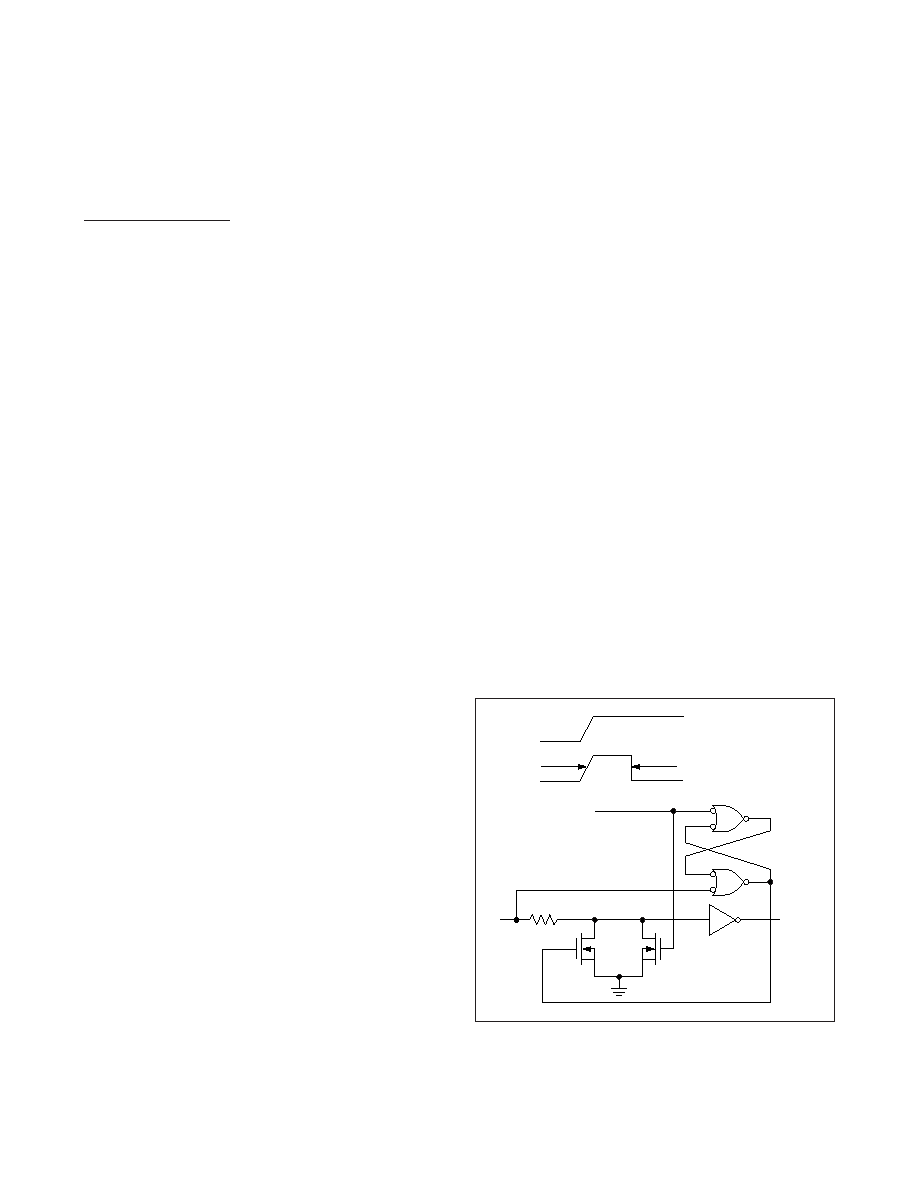
Hot-Swap Input Circuitry
The MAX3465/MAX3468 enable inputs feature hot-swap
capability. At the input there are two NMOS devices, M1
and M2 (Figure 4). When VCC ramps from 0, an internal
15s timer turns on M2 and sets the SR latch, which
also turns on M1. Transistors M2, a 2mA current sink,
and M1, a 100A current sink, pull DE to GND through a
5.6k
Ω resistor. M2 is designed to pull DE to the disabled
state against an external parasitic capacitance up to
100pF that can drive DE high. After 15s, the timer
deactivates M2 while M1 remains on, holding DE low
against three-state leakages that can drive DE high. M1
remains on until an external source overcomes the
required input current. At this time, the SR latch resets
and M1 turns off. When M1 turns off, DE reverts to a
standard, high-impedance CMOS input. Whenever VCC
drops below 1V, the hot-swap input is reset.
For RE there is a complementary circuit employing two
PMOS devices pulling to VCC.
VCC
TIMER
EN
DE
(HOT SWAP)
15
μs
100
μA
M1
M2
5.6k
Ω
2mA
Figure 4. Simplified Structure of the Driver Enable Pin (DE)
相关PDF资料 |
PDF描述 |
|---|---|
| HR10-10R-12S | RECEPTACLE W/SOCKET INSERT-12CON |
| VE-BW3-MX-F1 | CONVERTER MOD DC/DC 24V 75W |
| MAX1483ESA+ | IC TXRX RS485/RS422 LP 8-SOIC |
| VE-BW3-MW | CONVERTER MOD DC/DC 24V 100W |
| VE-BW2-MX-F4 | CONVERTER MOD DC/DC 15V 75W |
相关代理商/技术参数 |
参数描述 |
|---|---|
| MAX3465CSD+ | 功能描述:RS-422/RS-485 接口 IC 5V Fail-Safe 40Mbps Profibus Tcvr RoHS:否 制造商:Maxim Integrated 数据速率:1136 Kbps 工作电源电压:3 V to 5.5 V 电源电流:5.9 mA 工作温度范围:- 40 C to + 85 C 安装风格:SMD/SMT 封装 / 箱体:SOIC-28 封装:Tube |
| MAX3465CSD+T | 功能描述:RS-422/RS-485 接口 IC 5V Fail-Safe 40Mbps Profibus Tcvr RoHS:否 制造商:Maxim Integrated 数据速率:1136 Kbps 工作电源电压:3 V to 5.5 V 电源电流:5.9 mA 工作温度范围:- 40 C to + 85 C 安装风格:SMD/SMT 封装 / 箱体:SOIC-28 封装:Tube |
| MAX3465CSD-T | 功能描述:RS-422/RS-485 接口 IC RoHS:否 制造商:Maxim Integrated 数据速率:1136 Kbps 工作电源电压:3 V to 5.5 V 电源电流:5.9 mA 工作温度范围:- 40 C to + 85 C 安装风格:SMD/SMT 封装 / 箱体:SOIC-28 封装:Tube |
| MAX3465EPD | 功能描述:RS-422/RS-485 接口 IC RoHS:否 制造商:Maxim Integrated 数据速率:1136 Kbps 工作电源电压:3 V to 5.5 V 电源电流:5.9 mA 工作温度范围:- 40 C to + 85 C 安装风格:SMD/SMT 封装 / 箱体:SOIC-28 封装:Tube |
| MAX3465ESD | 功能描述:RS-422/RS-485 接口 IC RoHS:否 制造商:Maxim Integrated 数据速率:1136 Kbps 工作电源电压:3 V to 5.5 V 电源电流:5.9 mA 工作温度范围:- 40 C to + 85 C 安装风格:SMD/SMT 封装 / 箱体:SOIC-28 封装:Tube |
发布紧急采购,3分钟左右您将得到回复。