- 您现在的位置:买卖IC网 > PDF目录1939 > MAX350EAP (Maxim Integrated Products)IC MULTIPLEXER DUAL 4X1 20SSOP PDF资料下载
参数资料
| 型号: | MAX350EAP |
| 厂商: | Maxim Integrated Products |
| 文件页数: | 9/20页 |
| 文件大小: | 0K |
| 描述: | IC MULTIPLEXER DUAL 4X1 20SSOP |
| 产品培训模块: | Lead (SnPb) Finish for COTS Obsolescence Mitigation Program |
| 标准包装: | 66 |
| 功能: | 多路复用器 |
| 电路: | 2 x 4:1 |
| 导通状态电阻: | 100 欧姆 |
| 电压电源: | 单/双电源 |
| 电压 - 电源,单路/双路(±): | 2.7 V ~ 16 V,±2.7 V ~ 8 V |
| 电流 - 电源: | 1µA |
| 工作温度: | -40°C ~ 85°C |
| 安装类型: | 表面贴装 |
| 封装/外壳: | 20-SSOP(0.209",5.30mm 宽) |
| 供应商设备封装: | 20-SSOP |
| 包装: | 管件 |
Power-Supply Considerations
Overview
The MAX349/MAX350 construction is typical of most
CMOS analog switches. It has three supply pins: V+, V-
and GND. V+ and V- are used to drive the internal
CMOS switches, and they set the limits of the analog
voltage on any switch. Reverse ESD-protection diodes
are internally connected between each analog signal
pin and both V+ and V-. If any analog signal exceeds
V+ or V-, one of these diodes will conduct. During normal
operation, these (and other) reverse-biased ESD diodes
leak, forming the only current drawn from V+ or V-.
Virtually all the analog leakage current is through the
ESD diodes. Although the ESD diodes on a given sig-
nal pin are identical, and therefore fairly well balanced,
they are reverse biased differently. Each is biased by
either V+ or V- and the analog signal. This means their
leakages vary as the signal varies. The
difference in the
two diode leakages to the V+ and V- pins constitutes
the analog signal-path leakage current. All analog leak-
age current flows to the supply terminals, not to the
other switch terminal. This is why both sides of a given
switch can show leakage currents of either the same or
opposite polarity.
There is no connection between the analog signal
paths and GND.
V+ and GND power the internal logic and logic-level
translators, and set both the input and output logic lim-
its. The logic-level translators convert the logic levels to
switched V+ and V- signals to drive the analog signal
gates. This drive signal is the only connection between
the logic supplies (and signals) and the analog sup-
plies. V+ and V- have ESD-protection diodes to GND.
The logic-level inputs and output have ESD protection
to V+ and to GND.
The logic-level thresholds are CMOS and TTL compati-
ble when V+ is +5V. As V+ rises, the threshold increases
slightly. Therefore, when V+ reaches +12V, the threshold
is about 3.1V; above the TTL-guaranteed high-level mini-
mum of 2.8V, but still compatible with CMOS outputs.
MAX349/MAX350
Serially Controlled, Low-Voltage,
8-Channel/Dual 4-Channel Multiplexers
______________________________________________________________________________________
17
FOUR CLOCK
PULSES
DIN
SCLK
D4
SW4
D0
SW0
Figure 7. Differential Multiplexer Input Control
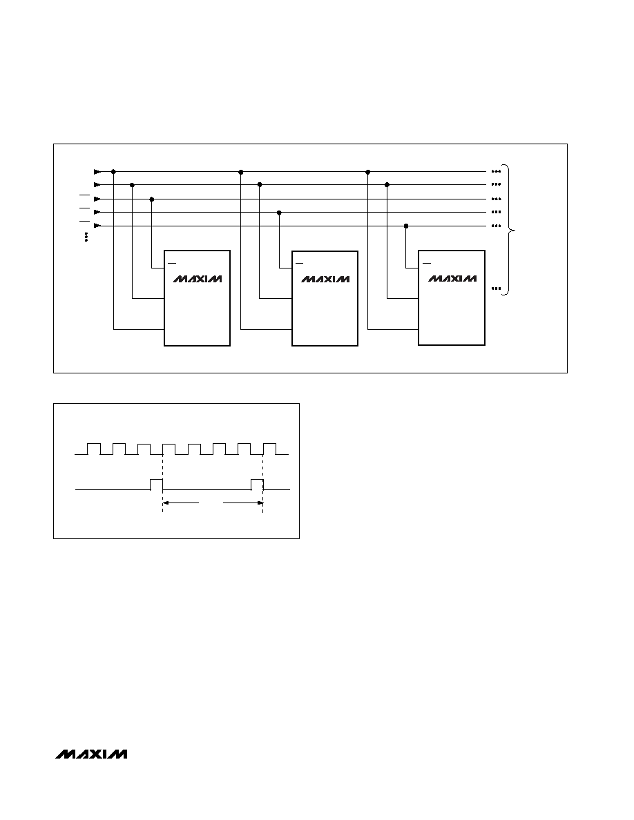
CS
SCLK
DIN
MAX349
MAX350
CS
SCLK
DIN
MAX349
MAX350
CS
SCLK
DIN
MAX349
MAX350
TO OTHER
SERIAL
DEVICES
DIN
SCLK
CS1
CS2
CS3
Figure 6. Addressable Serial Interface
相关PDF资料 |
PDF描述 |
|---|---|
| MAX351CSE-T | IC SWITCH QUAD SPST 16SOIC |
| MAX3535EEWI+T | IC TXRX RS485/422 28-SOIC |
| MAX355EPE | IC MULTIPLEXER DUAL 4X1 16DIP |
| MAX358EWE | IC MULTIPLEXER 8X1 16SOIC |
| MAX359EWE+T | IC MULTIPLEXER DUAL 4X1 16SOIC |
相关代理商/技术参数 |
参数描述 |
|---|---|
| MAX350EAP+ | 功能描述:多路器开关 IC 4:1 2Ch Low Voltage MUX RoHS:否 制造商:Texas Instruments 通道数量:1 开关数量:4 开启电阻(最大值):7 Ohms 开启时间(最大值): 关闭时间(最大值): 传播延迟时间:0.25 ns 工作电源电压:2.3 V to 3.6 V 工作电源电流: 最大工作温度:+ 85 C 安装风格:SMD/SMT 封装 / 箱体:UQFN-16 |
| MAX350EAP+T | 功能描述:多路器开关 IC 4:1 2Ch Low Voltage MUX RoHS:否 制造商:Texas Instruments 通道数量:1 开关数量:4 开启电阻(最大值):7 Ohms 开启时间(最大值): 关闭时间(最大值): 传播延迟时间:0.25 ns 工作电源电压:2.3 V to 3.6 V 工作电源电流: 最大工作温度:+ 85 C 安装风格:SMD/SMT 封装 / 箱体:UQFN-16 |
| MAX350EAP-T | 功能描述:多路器开关 IC RoHS:否 制造商:Texas Instruments 通道数量:1 开关数量:4 开启电阻(最大值):7 Ohms 开启时间(最大值): 关闭时间(最大值): 传播延迟时间:0.25 ns 工作电源电压:2.3 V to 3.6 V 工作电源电流: 最大工作温度:+ 85 C 安装风格:SMD/SMT 封装 / 箱体:UQFN-16 |
| MAX350EPN | 功能描述:多路器开关 IC RoHS:否 制造商:Texas Instruments 通道数量:1 开关数量:4 开启电阻(最大值):7 Ohms 开启时间(最大值): 关闭时间(最大值): 传播延迟时间:0.25 ns 工作电源电压:2.3 V to 3.6 V 工作电源电流: 最大工作温度:+ 85 C 安装风格:SMD/SMT 封装 / 箱体:UQFN-16 |
| MAX350EWN | 功能描述:多路器开关 IC RoHS:否 制造商:Texas Instruments 通道数量:1 开关数量:4 开启电阻(最大值):7 Ohms 开启时间(最大值): 关闭时间(最大值): 传播延迟时间:0.25 ns 工作电源电压:2.3 V to 3.6 V 工作电源电流: 最大工作温度:+ 85 C 安装风格:SMD/SMT 封装 / 箱体:UQFN-16 |
发布紧急采购,3分钟左右您将得到回复。