- 您现在的位置:买卖IC网 > PDF目录11320 > MAX350EWN+ (Maxim Integrated Products)IC MULTIPLEXER DUAL 4X1 18SOIC PDF资料下载
参数资料
| 型号: | MAX350EWN+ |
| 厂商: | Maxim Integrated Products |
| 文件页数: | 6/20页 |
| 文件大小: | 0K |
| 描述: | IC MULTIPLEXER DUAL 4X1 18SOIC |
| 产品培训模块: | Lead (SnPb) Finish for COTS Obsolescence Mitigation Program |
| 标准包装: | 40 |
| 功能: | 多路复用器 |
| 电路: | 2 x 4:1 |
| 导通状态电阻: | 100 欧姆 |
| 电压电源: | 单/双电源 |
| 电压 - 电源,单路/双路(±): | 2.7 V ~ 16 V,±2.7 V ~ 8 V |
| 电流 - 电源: | 1µA |
| 工作温度: | -40°C ~ 85°C |
| 安装类型: | 表面贴装 |
| 封装/外壳: | 18-SOIC(0.295",7.50mm 宽) |
| 供应商设备封装: | 18-SOIC W |
| 包装: | 管件 |
MAX349/MAX350
Serially Controlled, Low-Voltage,
8-Channel/Dual 4-Channel Multiplexers
14
______________________________________________________________________________________
Detailed Description
Basic Operation
The MAX349/MAX350 are 8-channel and dual 4-chan-
nel, serially controlled multiplexers (muxes). These
muxes are unusual in that any, all, or none of the input
channels can be directed to the output. All switches
are bidirectional, so inputs and outputs are inter-
changeable. When multiple inputs are connected to an
output, they are also connected to one another, sepa-
rated from each other only by the on-resistance of two
switches. Both parts require eight bits of serial data to
set all eight switches.
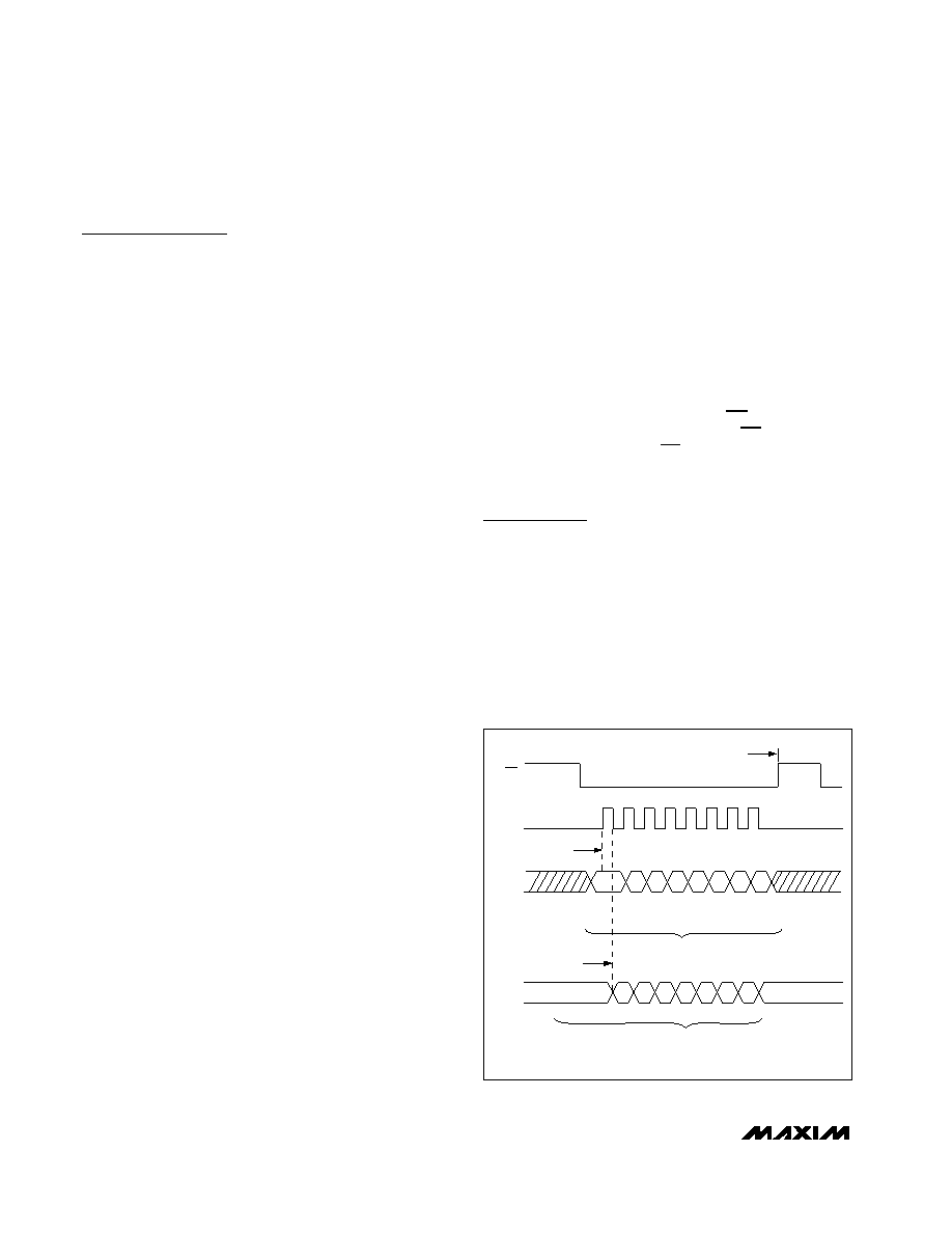
Serial Digital Interface
The MAX349/MAX350 interface can be thought of as an
8-bit shift register controlled by CS (Figure 2). While CS
is low, input data appearing at DIN is clocked into the
shift register synchronously with SCLK’s rising edge.
The input is an 8-bit word, each bit controlling one of
the eight switches (Tables 1 and 2). DOUT is the output
of the shift register, with data appearing synchronously
with SCLK’s falling edge. Data at DOUT is simply the
input data delayed by eight clock cycles.
When shifting the input data, D7 is the first bit in and
out of the shift register. While shifting data, the switches
remain in their previous configuration. When the eight
bits of data have been shifted in, CS is driven high.
This updates the new switch configuration and inhibits
further data from entering the shift register. Transitions
at DIN and SCLK have no effect when CS is high, and
DOUT holds the first input bit (D7) at its output.
More or fewer than eight clock cycles can be entered
during the CS low period. When this happens, the shift
register contains only the last eight serial data bits,
regardless of when they were entered. On the rising
edge of CS, all switches are set to the corresponding
states.
The MAX349/MAX350 three-wire serial interface is
compatible with SPI, QSPI, and MICROWIRE standards.
If interfacing with a Motorola processor serial interface,
set CPOL = 0. The MAX349/MAX350 are considered to
be slave devices (Figures 2 and 3). At power-up, the
shift register contains all zeros, and all switches are off.
The latch that drives the analog switch is updated on
the rising edge of CS, regardless of SCLK’s state. This
meets all SPI and QSPI requirements.
Daisy-Chaining
For a simple interface using several MAX349s and
MAX350s, “daisy-chain” the shift registers as shown in
Figure 5. The CS pins of all devices are connected,
and a stream of data is shifted through the MAX349s or
MAX350s in series. When CS is brought high, all
switches are updated simultaneously. Additional shift
registers may be included anywhere in series with the
MAX349/MAX350 data chain. Note that the DOUT high
level is V+, which may not be compatible with
TTL/CMOS devices if V+ differs from the logic supply
for these other devices.
Addressable Serial Interface
When several serial devices are configured as slaves,
addressable by the processor, DIN pins of each
decode logic individually control CS of each slave
device. When a slave is selected, its CS pin is driven
low, data is shifted in, and CS is driven high to latch the
data. Typically, only one slave is addressed at a time.
DOUT is not used.
Applications Information
8x1 Multiplexer
The MAX349 can be programmed normally, with only
one channel selected for every eight clock pulses, or it
can be programmed in a fast mode, where channel
changing occurs on each clock pulse.
In fast mode, select the channels by sending a single high
pulse (corresponding to the selected channel) at DIN, and
a corresponding CS low pulse for every eight clock puls-
es. As SCLK clocks this through the register, each switch
sequences one channel at a time, starting with channel 0.
D7
D6
D5 D4
MSB
LSB
D3 D2 D1 D0
DATA BITS FROM PREVIOUS DATA INPUT
DOUT POWER-UP DEFAULT: D7–D0 = 0
D6 D5 D4 D3 D2 D1 D0
D7
DOUT
DIN
SCLK
SWITCHES UPDATED
DATA CLOCKED IN
DATA CLOCKED OUT
CS
D7
INPUT DATA BITS
Figure 2. 3-Wire Interface Timing
相关PDF资料 |
PDF描述 |
|---|---|
| MAX351ESE+ | IC SWITCH QUAD SPST 16SOIC |
| MAX4661CPE+ | IC SWITCH QUAD SPST 16DIP |
| MAX4661CWE+ | IC SWITCH QUAD SPST 16SOIC |
| MAX4601CPE+ | IC SWITCH QUAD SPST 16DIP |
| DG528CWN+ | IC MULTIPLEXER 8X1 18SOIC |
相关代理商/技术参数 |
参数描述 |
|---|---|
| MAX350EWN+ | 功能描述:多路器开关 IC 4:1 2Ch Low Voltage MUX RoHS:否 制造商:Texas Instruments 通道数量:1 开关数量:4 开启电阻(最大值):7 Ohms 开启时间(最大值): 关闭时间(最大值): 传播延迟时间:0.25 ns 工作电源电压:2.3 V to 3.6 V 工作电源电流: 最大工作温度:+ 85 C 安装风格:SMD/SMT 封装 / 箱体:UQFN-16 |
| MAX350EWN+T | 功能描述:多路器开关 IC 4:1 2Ch Low Voltage MUX RoHS:否 制造商:Texas Instruments 通道数量:1 开关数量:4 开启电阻(最大值):7 Ohms 开启时间(最大值): 关闭时间(最大值): 传播延迟时间:0.25 ns 工作电源电压:2.3 V to 3.6 V 工作电源电流: 最大工作温度:+ 85 C 安装风格:SMD/SMT 封装 / 箱体:UQFN-16 |
| MAX350EWN-T | 功能描述:多路器开关 IC RoHS:否 制造商:Texas Instruments 通道数量:1 开关数量:4 开启电阻(最大值):7 Ohms 开启时间(最大值): 关闭时间(最大值): 传播延迟时间:0.25 ns 工作电源电压:2.3 V to 3.6 V 工作电源电流: 最大工作温度:+ 85 C 安装风格:SMD/SMT 封装 / 箱体:UQFN-16 |
| MAX350MJN | 功能描述:多路器开关 IC RoHS:否 制造商:Texas Instruments 通道数量:1 开关数量:4 开启电阻(最大值):7 Ohms 开启时间(最大值): 关闭时间(最大值): 传播延迟时间:0.25 ns 工作电源电压:2.3 V to 3.6 V 工作电源电流: 最大工作温度:+ 85 C 安装风格:SMD/SMT 封装 / 箱体:UQFN-16 |
| MAX35101EHJ+ | 制造商:Maxim Integrated Products 功能描述:TIME-TO-DIGITAL CONVERTER WITH AFE (BULK) - Rail/Tube 制造商:Maxim Integrated Products 功能描述:IC TIME-TO-DGTL CONV W/AFE TQFP |
发布紧急采购,3分钟左右您将得到回复。