- 您现在的位置:买卖IC网 > PDF目录10605 > MAX3535EEWI+ (Maxim Integrated Products)IC TXRX RS485/422 28-SOIC PDF资料下载
参数资料
| 型号: | MAX3535EEWI+ |
| 厂商: | Maxim Integrated Products |
| 文件页数: | 12/26页 |
| 文件大小: | 0K |
| 描述: | IC TXRX RS485/422 28-SOIC |
| 产品培训模块: | Lead (SnPb) Finish for COTS Obsolescence Mitigation Program |
| 标准包装: | 25 |
| 类型: | 收发器 |
| 驱动器/接收器数: | 1/1 |
| 规程: | RS422,RS485 |
| 电源电压: | 3 V ~ 5.5 V |
| 安装类型: | 表面贴装 |
| 封装/外壳: | 28-SOIC(0.295",7.50mm 宽) |
| 供应商设备封装: | 28-SOIC W |
| 包装: | 管件 |
| 产品目录页面: | 1408 (CN2011-ZH PDF) |
+3V to +5V, 2500VRMS Isolated RS-485/RS-422
Transceivers with ±15kV ESD Protection
ABSOLUTE MAXIMUM RATINGS
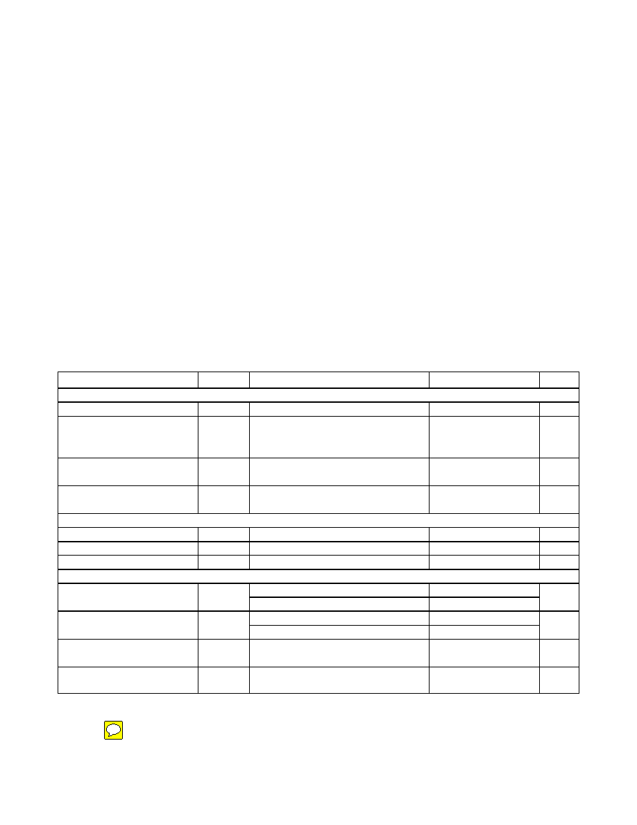
DC ELECTRICAL CHARACTERISTICS TABLE (MAX3535E)
(VCC1 = +3.0V to +5.5V, VCC2 = +3.13V to +7.5V, TA = -40°C to +85°C, unless otherwise noted. Typical values are at VCC1 = +3.3V,
VCC2 = +5V, TA = +25°C.)
Stresses beyond those listed under “Absolute Maximum Ratings” may cause permanent damage to the device. These are stress ratings only, and functional
operation of the device at these or any other conditions beyond those indicated in the operational sections of the specifications is not implied. Exposure to
absolute maximum rating conditions for extended periods may affect device reliability.
Logic Side—All Voltages Referenced to GND1.
VCC1 .........................................................................-0.3V to +6V
RE, DE, DI.................................................................-0.3V to +6V
RO1, ST1, ST2 ..........................................-0.3V to (VCC1 + 0.3V)
Isolated Side—All Voltages Referenced to GND2.
VCC2 .........................................................................-0.3V to +8V
SLO...........................................................-0.3V to (VCC2 + 0.3V)
A, B ......................................................................................±14V
RO2 .....................-0.3V to the lower of (VCC2 + 0.3V) and +3.4V
Y, Z ............................................................................-8V to +13V
Digital Outputs Maximum Current
RO1, RO2 .....................................................................±20mA
Y, Z Maximum Current .............................Short-Circuit Protected
ST1, ST2 Maximum Current............................................±300mA
Continuous Power Dissipation (TA = +70°C)
28-Pin Wide SO
(derate 9.5mW/°C above +70°C) .................................750mW
Operating Temperature Range
MXL1535ECWI, MAX3535ECWI .........................0°C to +70°C
MXL1535EEWI, MAX3535EEWI .......................-40°C to +85°C
Junction Temperature ......................................................+150°C
Storage Temperature Range .............................-65°C to +150°C
Lead Temperature (soldering, 10s) .................................+300°C
PARAMETER
SYMBOL
CONDITIONS
MIN
TYP
MAX
UNITS
LOGIC-SIDE SUPPLY (VCC1, GND1)
Logic-Side Supply Voltage
VCC1
3.0
5.5
V
Logic-Side Supply Current
ICC1
Transformer not driven, ST1 and ST2
unconnected, RE = low, DE = high,
fDATA = 0, RO1 = no load
5.9
13
mA
VCC1 Undervoltage-Lockout
Falling Trip
VUVL1
2.53
2.69
2.85
V
VCC1 Undervoltage-Lockout
Rising Trip
VUVH1
2.63
2.80
2.97
V
LOGIC INPUTS (DI, DE, RE)
Input High Voltage, DE, DI, RE
VIH
VIH is measured with respect to GND1
2.0
V
Input Low Voltage, DE, DI, RE
VIL
VIL is measured with respect to GND1
0.8
V
Logic-Side Input Current, DE, DI
IINC
±2A
LOGIC OUTPUTS (RO1, RE)
ISOURCE = 4mA, VCC1 = +4.5V
3.7
Receiver-Output High Voltage
(RO1)
VRO1H
ISOURCE = 4mA, VCC1 = +3V
2.4
V
ISINK = 4mA, VCC1 = +4.5V
0.4
Receiver-Output Low Voltage
(RO1)
VRO1L
ISINK = 4mA, VCC1 = +3V
0.4
V
Receiver-Output (RO1) Leakage
Current
IOZR
RE = high, VCC1 = +5.5V,
0
≤ VRO1 ≤ VCC1
±1
A
RE Low Output Current for Fault
Detect
IOL
RE = +0.4V, fault not asserted
40
60
80
A
MAX3535E/MXL1535E
2
Maxim Integrated
MAX3535E/MXL1535E
相关PDF资料 |
PDF描述 |
|---|---|
| RM12WBP-3S | CONN PLUG 3POS W/SOCKET INSERT |
| VE-B73-MX-F3 | CONVERTER MOD DC/DC 24V 75W |
| MAX3162CAI+ | IC TXRX RS232/485/422 28SSOP |
| RM12WBP-2S | CONN PLUG 2POS W/SOCKET INSERT |
| ADS62P45IRGCT | IC ADC 14BIT DUAL 125MSPS 64VQFN |
相关代理商/技术参数 |
参数描述 |
|---|---|
| MAX3535EEWI+ | 功能描述:RS-422/RS-485 接口 IC 3-5V 2500Vrms Iso Transceiver RoHS:否 制造商:Maxim Integrated 数据速率:1136 Kbps 工作电源电压:3 V to 5.5 V 电源电流:5.9 mA 工作温度范围:- 40 C to + 85 C 安装风格:SMD/SMT 封装 / 箱体:SOIC-28 封装:Tube |
| MAX3535EEWI+T | 功能描述:RS-422/RS-485 接口 IC 3-5V 2500Vrms Iso Transceiver RoHS:否 制造商:Maxim Integrated 数据速率:1136 Kbps 工作电源电压:3 V to 5.5 V 电源电流:5.9 mA 工作温度范围:- 40 C to + 85 C 安装风格:SMD/SMT 封装 / 箱体:SOIC-28 封装:Tube |
| MAX3535EEWI-T | 功能描述:RS-422/RS-485 接口 IC RoHS:否 制造商:Maxim Integrated 数据速率:1136 Kbps 工作电源电压:3 V to 5.5 V 电源电流:5.9 mA 工作温度范围:- 40 C to + 85 C 安装风格:SMD/SMT 封装 / 箱体:SOIC-28 封装:Tube |
| MAX3535EVKIT | 功能描述:RS-422/RS-485 接口 IC 3V to 5V Isolated RS485/RS422 Transceiver RoHS:否 制造商:Maxim Integrated 数据速率:1136 Kbps 工作电源电压:3 V to 5.5 V 电源电流:5.9 mA 工作温度范围:- 40 C to + 85 C 安装风格:SMD/SMT 封装 / 箱体:SOIC-28 封装:Tube |
| MAX3535EWI | 制造商:Maxim Integrated Products 功能描述:+3V TO +5V, 2500VRMS ISOLATED RS485/RS422 TRA - Rail/Tube |
发布紧急采购,3分钟左右您将得到回复。