- 您现在的位置:买卖IC网 > PDF目录2088 > MAX3679AETJ+T (Maxim Integrated Products)IC CLOCK GENERATOR LVPECL 32TQFN PDF资料下载
参数资料
| 型号: | MAX3679AETJ+T |
| 厂商: | Maxim Integrated Products |
| 文件页数: | 9/11页 |
| 文件大小: | 0K |
| 描述: | IC CLOCK GENERATOR LVPECL 32TQFN |
| 产品培训模块: | Lead (SnPb) Finish for COTS Obsolescence Mitigation Program |
| 标准包装: | 2,500 |
| 类型: | 时钟发生器,扇出配送,多路复用器 |
| PLL: | 带旁路 |
| 输入: | LVCMOS,LVTTL |
| 输出: | LVCMOS,LVPECL |
| 电路数: | 1 |
| 比率 - 输入:输出: | 2:4 |
| 差分 - 输入:输出: | 无/是 |
| 频率 - 最大: | 625MHz |
| 除法器/乘法器: | 是/是 |
| 电源电压: | 3 V ~ 3.6 V |
| 工作温度: | -40°C ~ 85°C |
| 安装类型: | 表面贴装 |
| 封装/外壳: | 32-WFQFN 裸露焊盘 |
| 供应商设备封装: | 32-TQFN-EP(5x5) |
| 包装: | 带卷 (TR) |
MAX3679A
Detailed Description
The MAX3679A is a low-jitter clock generator designed
to operate at Ethernet frequencies. It consists of an on-
chip crystal oscillator, PLL, programmable dividers,
LVCMOS output buffer, and LVPECL output buffers.
Using a low-frequency clock (crystal or CMOS input) as
a reference, the internal PLL generates a high-frequen-
cy output clock with excellent jitter performance.
Crystal Oscillator
An integrated oscillator provides the low-frequency
reference clock for the PLL. This oscillator requires an
external crystal connected between X_IN and X_OUT.
Crystal frequency is 25MHz.
REF_IN Buffer
An LVCMOS-compatible clock source can be connected
to REF_IN to serve as the reference clock.
The LVCMOS REF_IN buffer is internally biased to allow
AC- or DC-coupling. It is designed to operate up to
320MHz.
PLL
The PLL takes the signal from the crystal oscillator or
reference clock input and synthesizes a low-jitter, high-
frequency clock. The PLL contains a phase-frequency
detector (PFD), a lowpass filter, and a 625MHz voltage-
controlled oscillator (VCO). The VCO output is connect-
ed to the PFD input through a feedback divider. The
PFD compares the reference frequency to the divided-
down VCO output (fVCO/25) and generates a control
signal that keeps the VCO locked to the reference
clock. The high-frequency VCO output clock is sent to
the output dividers. To minimize noise-induced jitter,
the VCO supply (VCCA) is isolated from the core logic
and output buffer supplies.
Output Dividers
The output divider is programmable to allow a range of
output frequencies. See Table 2 for the divider input
settings. The output dividers are automatically set to
divide by 1 when the MAX3679A is in bypass mode
(BYPASS = 0).
LVPECL Drivers
The high-frequency outputs—QA, QB0, and QB1—are
differential PECL buffers designed to drive transmission
lines terminated with 50
Ω to VCC - 2.0V. The maximum
operating frequency is specified up to 320MHz. Each
output can be individually disabled, if not used. The
outputs go to a logic 0 when disabled.
LVCMOS Driver
QA_C, the LVCMOS output, is designed to drive a sin-
gle-ended high-impedance load. The maximum operat-
ing frequency is specified up to 160MHz. This output
can be disabled by the QAC_OE pin if not used and
goes to a high impedance when disabled.
Reset Logic/POR
During power-on, the power-on reset (POR) signal is
generated to synchronize all dividers. An external mas-
ter reset (MR) signal is not required.
Applications Information
Power-Supply Filtering
The MAX3679A is a mixed analog/digital IC. The PLL
contains analog circuitry susceptible to random noise.
In addition to excellent on-chip power-supply noise
rejection, the MAX3679A provides a separate power-
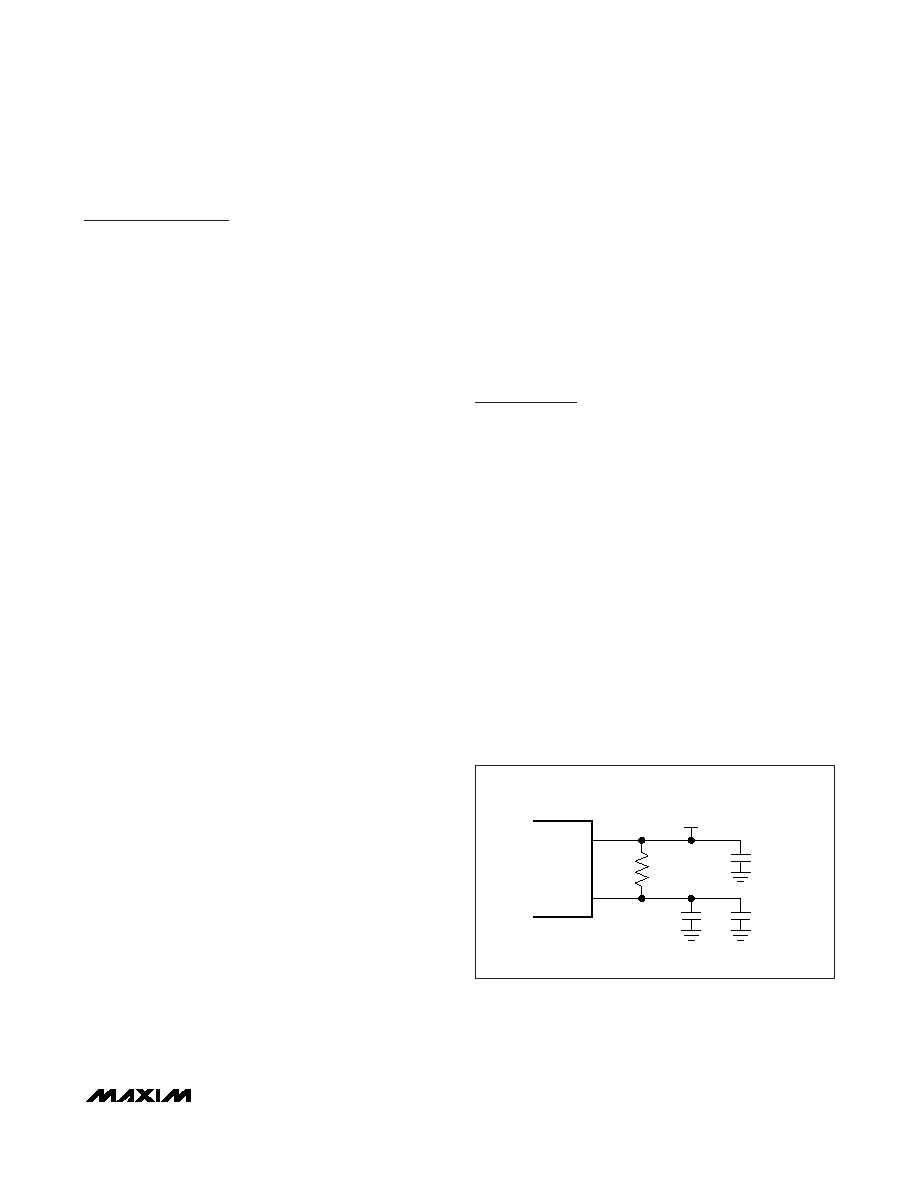
supply pin, VCCA, for the VCO circuitry. Figure 2 illus-
trates the recommended power-supply filter network for
VCCA. The purpose of this design technique is to
ensure clean input power supply to the VCO circuitry
and to improve the overall immunity to power-supply
noise. This network requires that the power supply is
+3.3V ±5%. Decoupling capacitors should be used on
all other supply pins for best performance.
Output Divider Configuration
Table 2 shows the input settings required to set the out-
put dividers. Leakage in the OPEN case must be less
than 1A. Note that when the MAX3679A is in bypass
mode (BYPASS set low), the output dividers are auto-
matically set to divide by 1.
VCC
VCCA
10.5
Ω
+3.3V
±5%
0.1
μF
10
μF
0.1
μF
Figure 2. Analog Supply Filtering
+3.3V, Low-Jitter Crystal to LVPECL
Clock Generator
_______________________________________________________________________________________
7
相关PDF资料 |
PDF描述 |
|---|---|
| MAX3747EUB+T | IC AMP LIMITING SFP 10-UMAX |
| MAX3761EEP+T | IC AMP LIMITING 622MBPS 20-QSOP |
| MAX3815ACCM+T | IC DGTL VIDEO EQUALIZER 48TQFP |
| MAX3815CCM+DG05 | IC EQUALIZER VIDEO 48-TQFP |
| MAX3816ACUE+T | IC I2C 2WIRE EXTENDER 16-TSSOP |
相关代理商/技术参数 |
参数描述 |
|---|---|
| MAX3679AEVKIT+ | 功能描述:时钟和定时器开发工具 Not Available From Mouser RoHS:否 制造商:Texas Instruments 产品:Evaluation Modules 类型:Clock Conditioners 工具用于评估:LMK04100B 频率:122.8 MHz 工作电源电压:3.3 V |
| MAX3679CTJ+ | 功能描述:时钟发生器及支持产品 3.3V Low-Jitter Crystal to LVPECL RoHS:否 制造商:Silicon Labs 类型:Clock Generators 最大输入频率:14.318 MHz 最大输出频率:166 MHz 输出端数量:16 占空比 - 最大:55 % 工作电源电压:3.3 V 工作电源电流:1 mA 最大工作温度:+ 85 C 安装风格:SMD/SMT 封装 / 箱体:QFN-56 |
| MAX3679CTJ+T | 功能描述:时钟发生器及支持产品 3.3V Low-Jitter Crystal to LVPECL RoHS:否 制造商:Silicon Labs 类型:Clock Generators 最大输入频率:14.318 MHz 最大输出频率:166 MHz 输出端数量:16 占空比 - 最大:55 % 工作电源电压:3.3 V 工作电源电流:1 mA 最大工作温度:+ 85 C 安装风格:SMD/SMT 封装 / 箱体:QFN-56 |
| MAX367C/D | 功能描述:TVS二极管阵列 Signal-Line Circuit Protector RoHS:否 制造商:Littelfuse 极性: 通道:4 Channels 击穿电压: 钳位电压:11.5 V 工作电压:2.5 V 峰值浪涌电流:20 A 安装风格:SMD/SMT 端接类型:SMD/SMT 系列: 最小工作温度:- 40 C 最大工作温度:+ 85 C |
| MAX367C/D+ | 功能描述:TVS二极管阵列 RoHS:否 制造商:Littelfuse 极性: 通道:4 Channels 击穿电压: 钳位电压:11.5 V 工作电压:2.5 V 峰值浪涌电流:20 A 安装风格:SMD/SMT 端接类型:SMD/SMT 系列: 最小工作温度:- 40 C 最大工作温度:+ 85 C |
发布紧急采购,3分钟左右您将得到回复。