- 您现在的位置:买卖IC网 > PDF目录98009 > MAX3679CTJ+ (MAXIM INTEGRATED PRODUCTS INC) 625 MHz, OTHER CLOCK GENERATOR, QCC32 PDF资料下载
参数资料
| 型号: | MAX3679CTJ+ |
| 厂商: | MAXIM INTEGRATED PRODUCTS INC |
| 元件分类: | 时钟产生/分配 |
| 英文描述: | 625 MHz, OTHER CLOCK GENERATOR, QCC32 |
| 封装: | 5 X 5 MM, 0.80 MM HEIGHT, ROHS COMPLIANT, MO-220WHHD-2, TQFN-32 |
| 文件页数: | 8/11页 |
| 文件大小: | 390K |
| 代理商: | MAX3679CTJ+ |
MAX3679
+3.3V, Low-Jitter Crystal to LVPECL
Clock Generator
6
_______________________________________________________________________________________
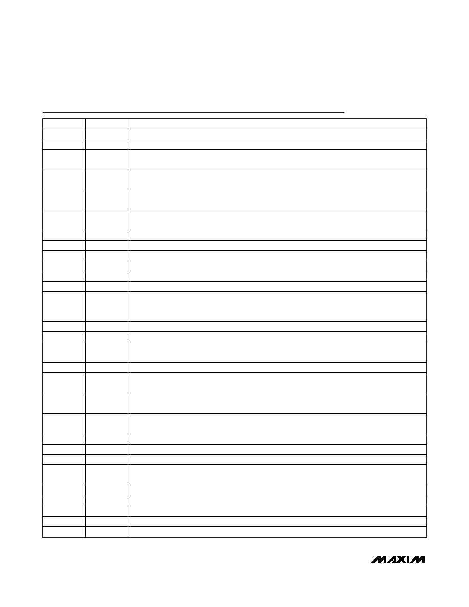
Pin Description
PIN
NAME
FUNCTION
1
VCCO_B
Power Supply for QB0 and QB1 Clock Outputs. Connect to +3.3V.
2, 19, 24
GND
Supply Ground
3
QB0_OE
LVCMOS/LVTTL Input. Enables/disables QB0 clock output. Connect pin high to enable LVPECL
clock output QB0. Connect low to set QB0 to a logic 0. Has internal 50k
input impedance.
4, 5
SELB1,
SELB0
LVCMOS/LVTTL Input. Controls NB divider setting. Has 50k
input impedance. See Table 2 for
more information.
6
QAC_OE
LVCMOS/LVTTL Input. Enables/disables QA_C clock output. Connect pin high to enable QA_C.
Connect low to set QA_C to a high-impedance state. Has internal 75k
pullup to VCC.
7
MR
LVCMOS/LVTTL Input. Master reset input. Pulse high for > 1μs to reset all dividers. Has internal
75k
pulldown to GND. Not required for normal operation.
8
GNDO_A
Ground for QA_C Output. Connect to supply ground.
9
QA_C
LVCMOS Clock Output
10
VDDO_A
Power Supply for QA_C Clock Output. Connect to +3.3V.
11
VCCO_A
Power Supply for QA Clock Output. Connect to +3.3V.
12
QA
Noninverting Clock Output, LVPECL
13
QA
Inverting Clock Output, LVPECL
14
BYPASS
LVCMOS/LVTTL Input (Active Low). Connect low to bypass the internal PLL. Connect high for
normal operation. When in bypass mode the output dividers are set to divide by 1. Has internal
75k
pullup to VCC.
15
RES1
Not Internally Connected. Connect to GND, VCC, or leave open for normal operation.
16
RES0
Reserved for Test. Connect to GND for normal operation.
17
VCCA
Analog Power Supply for the VCO. Connect to +3.3V. For additional power-supply noise filtering,
this pin can connect to VCC through 10.5
as shown in Figure 2 (requires VCC = +3.3V ±5%).
18
VCC
Core Power Supply. Connect to +3.3V.
20
QA_OE
LVCMOS/LVTTL Input. Enables/disables the QA clock output. Connect this pin high to enable the
LVPECL clock output QA. Connect low to set QA to a logic 0. Has internal 75k
pullup to VCC.
21, 22
SELA0,
SELA1
LVCMOS/LVTTL Input. Controls NA divider setting. See Table 2 for more information. Has 50k
input impedance.
23
QB1_OE
LVCMOS/LVTTL Input. Enables/disables QB1 clock output. Connect pin high to enable LVPECL
clock output QB1. Connect low to set QB1 to a logic 0. Has internal 50k
input impedance.
25
X_OUT
Crystal Oscillator Output
26
X_IN
Crystal Oscillator Input
27
REF_IN
LVCMOS Reference Clock Input. Self-biased to allow AC- or DC-coupling.
28
IN_SEL
LVCMOS/LVTTL Input. Connect high or leave open to use a crystal. Connect low to use REF_IN.
Has internal 75k
pullup to VCC.
29
QB1
LVPECL, Inverting Clock Output
30
QB1
LVPECL, Noninverting Clock Output
31
QB0
LVPECL, Inverting Clock Output
32
QB0
LVPECL, Noninverting Clock Output
—
EP
Exposed Pad. Connect to supply ground for proper electrical and thermal performance.
相关PDF资料 |
PDF描述 |
|---|---|
| MAX7329AUP+ | 8 I/O, PIA-GENERAL PURPOSE, PDSO20 |
| MAX7329AAP+ | 8 I/O, PIA-GENERAL PURPOSE, PDSO20 |
| MAXQ3212-EMX+ | 16-BIT, EEPROM, 3.58 MHz, RISC MICROCONTROLLER, PDIP24 |
| MAXQ613E-0000+ | 16-BIT, FLASH, 12 MHz, RISC MICROCONTROLLER, PQFP32 |
| MAXQ613K-0000+ | 16-BIT, FLASH, 12 MHz, RISC MICROCONTROLLER, PQFP44 |
相关代理商/技术参数 |
参数描述 |
|---|---|
| MAX3679CTJ+ | 功能描述:时钟发生器及支持产品 3.3V Low-Jitter Crystal to LVPECL RoHS:否 制造商:Silicon Labs 类型:Clock Generators 最大输入频率:14.318 MHz 最大输出频率:166 MHz 输出端数量:16 占空比 - 最大:55 % 工作电源电压:3.3 V 工作电源电流:1 mA 最大工作温度:+ 85 C 安装风格:SMD/SMT 封装 / 箱体:QFN-56 |
| MAX3679CTJ+T | 功能描述:时钟发生器及支持产品 3.3V Low-Jitter Crystal to LVPECL RoHS:否 制造商:Silicon Labs 类型:Clock Generators 最大输入频率:14.318 MHz 最大输出频率:166 MHz 输出端数量:16 占空比 - 最大:55 % 工作电源电压:3.3 V 工作电源电流:1 mA 最大工作温度:+ 85 C 安装风格:SMD/SMT 封装 / 箱体:QFN-56 |
| MAX367C/D | 功能描述:TVS二极管阵列 Signal-Line Circuit Protector RoHS:否 制造商:Littelfuse 极性: 通道:4 Channels 击穿电压: 钳位电压:11.5 V 工作电压:2.5 V 峰值浪涌电流:20 A 安装风格:SMD/SMT 端接类型:SMD/SMT 系列: 最小工作温度:- 40 C 最大工作温度:+ 85 C |
| MAX367C/D+ | 功能描述:TVS二极管阵列 RoHS:否 制造商:Littelfuse 极性: 通道:4 Channels 击穿电压: 钳位电压:11.5 V 工作电压:2.5 V 峰值浪涌电流:20 A 安装风格:SMD/SMT 端接类型:SMD/SMT 系列: 最小工作温度:- 40 C 最大工作温度:+ 85 C |
| MAX367CPN | 功能描述:TVS二极管阵列 RoHS:否 制造商:Littelfuse 极性: 通道:4 Channels 击穿电压: 钳位电压:11.5 V 工作电压:2.5 V 峰值浪涌电流:20 A 安装风格:SMD/SMT 端接类型:SMD/SMT 系列: 最小工作温度:- 40 C 最大工作温度:+ 85 C |
发布紧急采购,3分钟左右您将得到回复。