- 您现在的位置:买卖IC网 > PDF目录5333 > MAX367CWN+ (Maxim Integrated Products)IC SIGNAL-LINE CIRC PROT 18-SOIC PDF资料下载
参数资料
| 型号: | MAX367CWN+ |
| 厂商: | Maxim Integrated Products |
| 文件页数: | 7/12页 |
| 文件大小: | 0K |
| 描述: | IC SIGNAL-LINE CIRC PROT 18-SOIC |
| 产品培训模块: | Lead (SnPb) Finish for COTS Obsolescence Mitigation Program |
| 标准包装: | 40 |
| 电压 - 箝位: | ±40V |
| 技术: | 混合技术 |
| 功率(瓦特): | 762mW |
| 电路数: | 8 |
| 应用: | 通用 |
| 封装/外壳: | 18-SOIC(0.295",7.50mm 宽) |
| 供应商设备封装: | 18-SOIC W |
| 包装: | 管件 |
�� �
�
�Signal-Line� Circuit� Protectors�
�The� current� through� each� protector� should� never� exceed�
�30mA.� Always� calculate� the� power� dissipated� by� all� the�
�protectors� in� worst-case� conditions� (maximum� voltage�
�5�
�and� current� through� each� protector)� to� ensure� the� pack-�
�age� dissipation� limit� is� not� reached.�
�With� single-supply� operation,� grounded� loads� will� have�
�zero� voltage� (and� current)� whenever� the� input� voltage� is�
�below� approximately� 2V.� In� effect,� both� the� IN� and� OUT�
�pins� are� in� fault� condition.�
�A� special� case� arises� when� power� is� off:� The� part� is� in� a�
�perpetual� fault� condition� but� no� fault� current� flows�
�because� all� the� internal� FETs� are� off.�
�Single-Supply� Output� Operation�
�4�
�3�
�2�
�1�
�0�
�-1�
�-2�
�-3�
�-4�
�V+� =� +5V�
�V-� =� -5V�
�R� OUT� =� 100M� ?�
�Single-supply� operation� is� a� special� case.� Signals� can-�
�-30�
�-20�
�-10�
�0�
�10�
�20�
�30�
�not� go� to� ground,� since� from� 0V� to� approximately� +2V� is�
�a� fault� condition.�
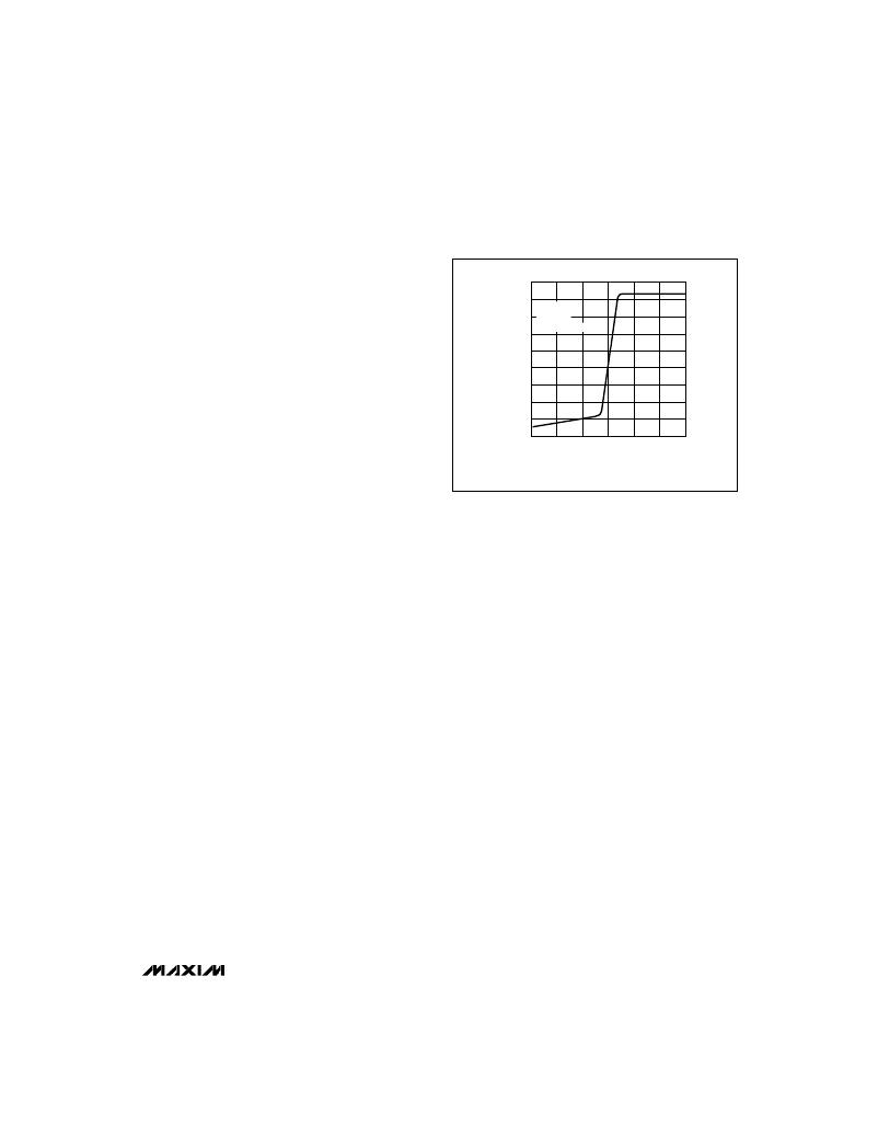
�Extremely� Low-Current� Operation�
�Figure� 3� shows� the� typical� high-impedance� transfer�
�characteristics� with� a� 100M� ?� load.� Compared� to� the�
�transfer� characteristic� at� 1M� ?� (see� Typical� Operating�
�Characteristics),� the� two� knees� are� closer� to� the� supply�
�voltages� and� the� slopes� of� the� flat� portions� of� the� curve�
�(fault� conditions)� are� steeper.� As� the� load� resistance� is�
�increased� even� further,� the� positive� and� negative� knees�
�increase,� and� the� slopes� in� fault� conditions� increase�
�even� more.� Eventually,� at� some� extremely� high� output�
�resistance� (e.g.,� Tera� ohms),� the� output� voltage� can�
�exceed� the� supply� voltage� during� fault� conditions.� This�
�is� due� to� extremely� low� leakage� currents� from� the� input�
�to� output.�
�When� the� protector’s� output� side� is� connected� to� very�
�high-resistance,� very� low-current� loads� (such� as� op-�
�amp� inputs),� a� small� leakage� current� flows� from� the�
�input� to� the� output� during� fault� conditions.� This� current�
�is� typically� below� a� nano-ampere� (<10� -9� A)� but,� if� the�
�output� resistance� is� high� enough,� it� can� cause� the� out-�
�put� voltage� to� exceed� the� supply� voltages� during� fault�
�conditions.�
�This� condition� can� be� self-correcting,� however,� if� the�
�high-resistance� load� has� protection� diodes� to� the� sup-�
�ply� rails� (either� external� or� internal� to� the� op� amp).�
�These� diodes� conduct� the� leakage� current� to� the� supply�
�rails� and� safely� limit� the� output� voltage.� An� alternative� is�
�to� add� a� high-value� resistor� to� ground� in� parallel� with�
�the� load.� This� resistor� may� be� as� low� as� 1000M� ?� ;� its�
�value� must� be� determined� experimentally� at� the� highest�
�anticipated� operational� temperature.�
�The� fault� protectors� will� not� normally� be� used� with� high-�
�impedance� FET-input� amplifiers� that� lack� input� protection�
�diodes.� Such� amplifiers� are� fragile� and� are� normally�
�INPUT� VOLTAGE� (V)�
�Figure� 3.� High-Impedance� Transfer� Characteristic�
�reserved� for� use� when� ultra-low� leakage� (pA)� is� needed.�
�The� MAX366/MAX367� have� nano-amperes� of� leakage,�
�which� would� negate� the� low� leakage� of� the� unprotected�
�amplifier.�
�Low-Voltage� Operation�
�The� MAX366/MAX367� “operate”� with� supply� voltages�
�all� the� way� down� to� 0V,� but� what� they� do� to� the� signal� is�
�not� obvious.� With� a� total� supply� voltage� of� 3.5V,� the�
�protector� is� in� a� fault� condition� with� nearly� any� input� that�
�is� not� close� to� 2.0V.� Below� 3.5V� (including� power� off),�
�the� protector� is� perpetually� in� a� fault� condition� (i.e.,� high�
�impedance).�
�When� the� supply� voltage(s)� ramps� up� (and/or� down)�
�from� zero,� the� signal� path� is� initially� in� a� fault� condition�
�(open),� until� the� supply� voltage� passes� the� input� volt-�
�age.� The� output� starts� at� zero� and� is� delayed� from�
�reaching� the� input� voltage� as� the� part� comes� out� of� the�
�fault� condition.� If� the� supply� voltage� exceeds� about�
�3.5V,� but� never� exceeds� the� input� voltage,� the� output�
�will� follow� the� supply,� always� remaining� about� 1.3V�
�below� the� positive� supply� voltage� or� 2V� above� the� neg-�
�ative� supply� voltage.� If� the� input� voltage� subsequently�
�comes� out� of� the� fault� condition,� the� output� returns� to�
�the� input� value.� This� set� of� conditions� is� exactly�
�reversed� when� power� ramps� down� to� zero.�
�Since� the� input� and� output� pins� are� identical� and� inter-�
�changeable,� predicting� whether� or� not� the� part� is� in� a�
�fault� condition� is� easy:� If� either� IN� or� OUT� exceeds� V+�
�or� V-,� a� fault� condition� exists� and� the� current� that� flows�
�will� be� just� enough� to� cause� the� other� signal� pin� (OUT�
�or� IN)� to� approach� the� appropriate� supply� rail.�
�_______________________________________________________________________________________�
�7�
�相关PDF资料 |
PDF描述 |
|---|---|
| CA3-B0-22-650-12A-D | CIRC BRKR SWITCH LEVER 3P 50A |
| NPPN222FFKS-RC | CONN RECEPT 2MM DUAL SMD 44POS |
| EL5374IU | IC AMP TRPL DIFF 550MHZ 28-QSOP |
| NPPN222FFKP-RC | CONN RECEPT 2MM DUAL SMD 44POS |
| MMH21-050 | CONN RACK/PANEL 50POS 5A |
相关代理商/技术参数 |
参数描述 |
|---|---|
| MAX367CWN+ | 功能描述:隔离器接口集成电路 Signal Line Circuit Protector RoHS:否 制造商:Texas Instruments 通道数量:2 传播延迟时间: 电源电压-最大:5.5 V 电源电压-最小:3 V 电源电流:3.6 mA 功率耗散: 最大工作温度:+ 125 C 安装风格: 封装 / 箱体:SOIC-8 封装:Tube |
| MAX367CWN+T | 功能描述:隔离器接口集成电路 Signal Line Circuit Protector RoHS:否 制造商:Texas Instruments 通道数量:2 传播延迟时间: 电源电压-最大:5.5 V 电源电压-最小:3 V 电源电流:3.6 mA 功率耗散: 最大工作温度:+ 125 C 安装风格: 封装 / 箱体:SOIC-8 封装:Tube |
| MAX367CWN-T | 功能描述:TVS二极管阵列 RoHS:否 制造商:Littelfuse 极性: 通道:4 Channels 击穿电压: 钳位电压:11.5 V 工作电压:2.5 V 峰值浪涌电流:20 A 安装风格:SMD/SMT 端接类型:SMD/SMT 系列: 最小工作温度:- 40 C 最大工作温度:+ 85 C |
| MAX367EPN | 功能描述:热插拔功率分布 RoHS:否 制造商:Texas Instruments 产品:Controllers & Switches 电流限制: 电源电压-最大:7 V 电源电压-最小:- 0.3 V 工作温度范围: 功率耗散: 安装风格:SMD/SMT 封装 / 箱体:MSOP-8 封装:Tube |
| MAX367EPN+ | 功能描述:热插拔功率分布 Signal Line Circuit Protector RoHS:否 制造商:Texas Instruments 产品:Controllers & Switches 电流限制: 电源电压-最大:7 V 电源电压-最小:- 0.3 V 工作温度范围: 功率耗散: 安装风格:SMD/SMT 封装 / 箱体:MSOP-8 封装:Tube |
发布紧急采购,3分钟左右您将得到回复。