- 您现在的位置:买卖IC网 > PDF目录5315 > MAX367CWN+T (Maxim Integrated Products)IC CIRC PROT SIGNAL-LINE 18-SOIC PDF资料下载
参数资料
| 型号: | MAX367CWN+T |
| 厂商: | Maxim Integrated Products |
| 文件页数: | 6/12页 |
| 文件大小: | 0K |
| 描述: | IC CIRC PROT SIGNAL-LINE 18-SOIC |
| 产品培训模块: | Lead (SnPb) Finish for COTS Obsolescence Mitigation Program |
| 标准包装: | 1,000 |
| 电压 - 箝位: | ±40V |
| 技术: | 混合技术 |
| 功率(瓦特): | 762mW |
| 电路数: | 8 |
| 应用: | 通用 |
| 封装/外壳: | 18-SOIC(0.295",7.50mm 宽) |
| 供应商设备封装: | 18-SOIC W |
| 包装: | 带卷 (TR) |
�� �
�
�Signal-Line� Circuit� Protectors�
�As� long� as� the� signal� is� within� these� limits,� all� three� tran-�
�sistors� conduct� and� a� low-resistance� path� is� maintained�
�from� the� IN� to� OUT� pin.� (Note� that,� since� the� device� is�
�symmetrical,� IN� and� OUT� pins� can� be� interchanged.)�
�When� the� signal� is� beyond� the� gate� threshold� of� either�
�Q2� or� Q1/Q3,� the� path� resistance� rises� dramatically.�
�When� power� is� off,� none� of� the� transistors� have� gate�
�bias,� so� the� circuit� from� IN� to� OUT� is� open.�
�Normal� Operation�
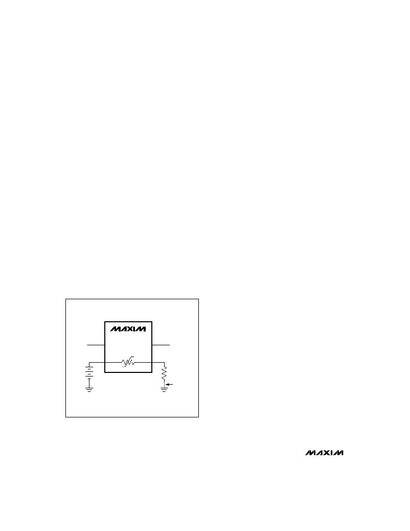
�In� normal� operation,� the� protector� is� placed� in� series�
�with� the� signal� line� and� the� power� supplies� are� con-�
�nected� to� V+� and� V-� (see� Figure� 2).� V-� is� ground� when�
�operating� with� a� single� supply.� When� power� is� applied,�
�each� protector� acts� as� a� resistor� in� the� signal� path.�
�Any� voltage� source� on� the� “input”� side� of� the� switch� will�
�be� conducted� through� the� protector� to� the� output.� (Note�
�that,� since� the� protector� is� symmetrical,� IN� and� OUT�
�pins� can� be� interchanged.)�
�If� the� output� load� is� resistive,� it� will� draw� current,� and� a�
�voltage� divider� will� be� formed� with� the� internal� resistance�
�so� the� output� voltage� will� be� lower� than� the� input� voltage.�
�Since� the� internal� resistance� is� typically� less� than� 100� ?� ,�
�high-impedance� loads� will� be� relatively� unaffected� by� the�
�presence� of� the� protector.� The� protector’s� path� resis-�
�tance� is� a� function� of� the� supply� voltage� and� the� signal�
�voltage� (see� Typical� Operating� Characteristics).�
�MAX366�
�Power� Off�
�When� power� is� off� (i.e.,� V+� =� V-� =� 0V),� the� protector� is� a�
�virtual� open� circuit,� and� all� voltages� on� each� side� are�
�isolated� from� each� other� up� to� ±40V.� With� ±40V� applied�
�to� the� input� pin,� the� output� pin� will� be� 0V,� regardless� of�
�its� resistance� to� ground.�
�Fault� Conditions�
�A� fault� condition� exists� when� the� voltage� on� either� sig-�
�nal� pin� is� within� about� 1.5V� of� either� supply� rail� or�
�exceeds� either� supply� rail.� This� definition� is� valid� when�
�power� is� applied� and� when� it� is� off,� as� well� as� during� all�
�the� states� as� power� ramps� up� or� down.�
�During� a� fault,� the� protector� acts� as� a� variable� resistor,�
�conducting� only� enough� to� sustain� the� other� side� of� the�
�switch� within� about� 1.5V� of� the� supply� rail.� This� voltage�
�is� known� as� the� “fault� knee� voltage,”� and� is� not� symmet-�
�rical.� It� is� approximately� 1.3V� down� from� the� positive�
�supply� (V+� pin)� or� approximately� 2.0V� up� from� the� neg-�
�ative� supply� (V-� pin).� Each� fault� knee� voltage� varies�
�slightly� with� supply� voltage,� with� output� current,� and�
�from� device� to� device.�
�During� a� fault� condition,� all� the� fault� current� flows�
�from� one� signal� pin� through� the� protector� and� out�
�the� other� signal� pin.� No� fault� current� flows� through�
�either� supply� pin.� (There� will� be� a� few� pico-amps� of�
�leakage� current� from� each� signal� pin� to� each� supply�
�pin,� but� this� is� independent� of� fault� current.)�
�During� the� fault� condition,� enough� current� will� flow� to�
�maintain� the� output� voltage� at� the� fault� knee� voltage,� so�
�the� fault� current� is� a� function� of� the� output� resistance�
�and� the� supply� voltage.� The� output� voltage� and� cur-�
�rent� have� the� same� polarity� as� the� fault.�
�The� maximum� input� fault� voltage� is� 40V� from� the� “oppo-�
�site-polarity� supply� rail.”� This� means� the� input� can� go�
�V-�
�4�
�V-�
�V+�
�8�
�V+�
�to� ±35V� with� ±5V� supplies� or� to� ±25V� with� ±15V� sup-�
�plies.� The� fault� voltage� is� highest� (±40V)� when� the� sup-�
�plies� are� off� (V+� =� V-� =� 0V).�
�V� IN�
�1�
�IN1�
�OUT1�
�7�
�V� OUT�
�Using� the� circuit� of� Figure� 2,� the� approximate� fault� cur-�
�rents� are� as� follows:�
�R� OUT�
�V� LOW�
�1)� For� positive� faults:�
�I� (F)� ≈� (V+� -� 1.3V� -� V� LOW� )� ÷� R� OUT�
�2)� For� negative� faults:�
�I� (F)� ≈� (V-� +� 2V� +� V� LOW� )� ÷� R� OUT�
�where� V� LOW� is� the� terminating� voltage� at� the� far� end� of�
�R� OUT� .� V� LOW� =� 0V� when� R� OUT� is� grounded.�
�Figure� 2.� Application� Circuit�
�6�
�_______________________________________________________________________________________�
�相关PDF资料 |
PDF描述 |
|---|---|
| MAX366ESA+T | IC CIRC PROT SIGNAL-LINE 8-SOIC |
| MAX6497ATA+T | IC CNTRLR PROT SW 8-TDFN |
| NPPN402GFNS-RC | CONN RECEPT 2MM DUAL SMD 80POS |
| MAX6498ATA+T | IC CNTRLR PROT SW 8-TDFN |
| MAX6397MATA+T | IC SW OVERVOLT PROT 8-TDFN |
相关代理商/技术参数 |
参数描述 |
|---|---|
| MAX367EPN | 功能描述:热插拔功率分布 RoHS:否 制造商:Texas Instruments 产品:Controllers & Switches 电流限制: 电源电压-最大:7 V 电源电压-最小:- 0.3 V 工作温度范围: 功率耗散: 安装风格:SMD/SMT 封装 / 箱体:MSOP-8 封装:Tube |
| MAX367EPN+ | 功能描述:热插拔功率分布 Signal Line Circuit Protector RoHS:否 制造商:Texas Instruments 产品:Controllers & Switches 电流限制: 电源电压-最大:7 V 电源电压-最小:- 0.3 V 工作温度范围: 功率耗散: 安装风格:SMD/SMT 封装 / 箱体:MSOP-8 封装:Tube |
| MAX367EWN | 功能描述:热插拔功率分布 RoHS:否 制造商:Texas Instruments 产品:Controllers & Switches 电流限制: 电源电压-最大:7 V 电源电压-最小:- 0.3 V 工作温度范围: 功率耗散: 安装风格:SMD/SMT 封装 / 箱体:MSOP-8 封装:Tube |
| MAX367EWN+ | 功能描述:热插拔功率分布 RoHS:否 制造商:Texas Instruments 产品:Controllers & Switches 电流限制: 电源电压-最大:7 V 电源电压-最小:- 0.3 V 工作温度范围: 功率耗散: 安装风格:SMD/SMT 封装 / 箱体:MSOP-8 封装:Tube |
| MAX367EWN+T | 功能描述:热插拔功率分布 RoHS:否 制造商:Texas Instruments 产品:Controllers & Switches 电流限制: 电源电压-最大:7 V 电源电压-最小:- 0.3 V 工作温度范围: 功率耗散: 安装风格:SMD/SMT 封装 / 箱体:MSOP-8 封装:Tube |
发布紧急采购,3分钟左右您将得到回复。