- 您现在的位置:买卖IC网 > PDF目录10609 > MAX3804ETE#G16 (Maxim Integrated Products)IC EQUALIZER REC 12.5GBPS 16TQFN PDF资料下载
参数资料
| 型号: | MAX3804ETE#G16 |
| 厂商: | Maxim Integrated Products |
| 文件页数: | 2/9页 |
| 文件大小: | 0K |
| 描述: | IC EQUALIZER REC 12.5GBPS 16TQFN |
| 产品培训模块: | Lead (SnPb) Finish for COTS Obsolescence Mitigation Program |
| 标准包装: | 100 |
| 类型: | 发射器 |
| 规程: | 以太网 |
| 电源电压: | 3 V ~ 3.6 V |
| 安装类型: | 表面贴装 |
| 封装/外壳: | 16-WFQFN 裸露焊盘 |
| 供应商设备封装: | 16-TQFN-EP(3x3) |
| 包装: | 管件 |
| 产品目录页面: | 1408 (CN2011-ZH PDF) |
MAX3804
12.5Gbps Settable Receive Equalizer
2
_______________________________________________________________________________________
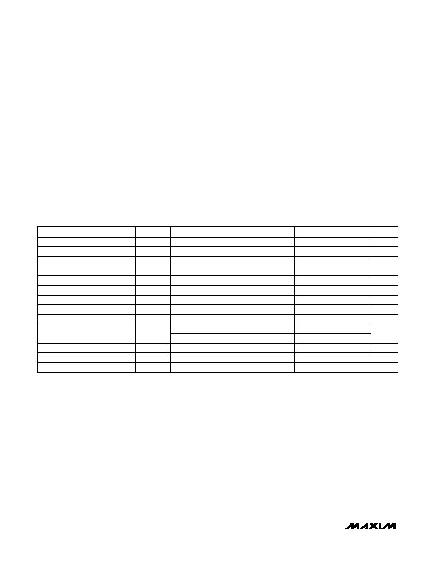
ABSOLUTE MAXIMUM RATINGS
ELECTRICAL CHARACTERISTICS
(VCC = +3.0V to +3.6V, VCC1 = VCC2 = +1.65V to +3.6V, TA = -40°C to +85°C. Typical values are at VCC = VCC1 = VCC2 = +3.3V,
and TA = +25°C, unless otherwise noted.)
Stresses beyond those listed under “Absolute Maximum Ratings” may cause permanent damage to the device. These are stress ratings only, and functional
operation of the device at these or any other conditions beyond those indicated in the operational sections of the specifications is not implied. Exposure to
absolute maximum rating conditions for extended periods may affect device reliability.
Supply Voltage (VCC) ............................................-0.5V to +4.0V
CML Supply Voltage (VCC1, VCC2) ............-0.5V to (VCC + 0.5V)
Current at Serial Output (SDO+, SDO-) ............................
±25mA
Input Voltage (SDI+, SDI-, EQ1,
EQ2, EQ3) ..............................................-0.5V to (VCC + 0.5V)
Continuous Power Dissipation (TA = +85°C)
16-Lead Thin QFN-EP (derate 17.5mW/
°C
above +85°C) ........................................................1398mW
Operating Temperature Range ...........................-40°C to +85°C
Storage Temperature Range .............................-55°C to +150°C
Lead Temperature (soldering, 10s) .................................+300°C
PARAMETER
SYMBOL
CONDITIONS
MIN
TYP
MAX
UNITS
Supply Current
ICC
35
50
mA
CML Input Differential
VIN
AC-coupled or DC-coupled (Note 1)
400
1200
mVP-P
CML Input Common Mode
DC-coupled
VCC1
- 0.4
VCC1
+ 0.1
V
CML Input Termination
Single ended
42.5
50
57.5
CML Input Return Loss
Up to 5GHz
10
dB
CML Output Differential
VOUT
400
500
600
mVP-P
CML Output Impedance
Single ended
42.5
50
57.5
CML Output Transition Time
tR, tF
20% to 80% (Notes 2, 6)
35
ps
At 10.7Gbps (Notes 3, 4, 5, 6)
24
30
Residual Jitter Output
(Total RJ, PWD, and PDJ)
At 12.5Gbps (Notes 3, 4, 5, 6)
17
30
psP-P
LVTTL Input Current
IIH, IIL
-30
+30
A
LVTTL Input Low
VIL
0.8
V
LVTTL Input High
VIH
2.0
V
Note 1: Differential Input Sensitivity is defined at the input to a transmission line. The transmission line is differential Z0 = 100
, 6-mil
microstrip in FR-4,
εr = 4.5, and tan δ = 0.02, VIN = (SDI+ - SDI-).
Note 2: Measured with 0000011111 pattern at 12.5Gbps.
Note 3: Residual jitter is the difference in total jitter (RJ, PWD, and PDJ) between the transmitted signal (at the input to the transmis-
sion line) and equalizer output. Total residual jitter is DJP-P + 14.2 x RJRMS.
Note 4: Measured at 10.7Gbps using a pattern of 100 ones, 27PRBS, 100 zeros, 27PRBS, and at 12.5Gbps using a K28.5 pattern.
Deterministic jitter at the input is from frequency-dependent, media-induced loss only.
Note 5: VIN = 400mVP-P to 1200mVP-P, input path is 0 to 30in, 6-mil microstrip in FR-4,
εr = 4.5, and tan δ = 0.02.
Note 6: Guaranteed by design and characterization.
相关PDF资料 |
PDF描述 |
|---|---|
| VE-25K-MX | CONVERTER MOD DC/DC 40V 75W |
| 18882-4SG-522 | CONN RCPT 4POS CABLE SKT |
| VE-25J-MX | CONVERTER MOD DC/DC 36V 75W |
| MAX3237EAI+ | IC TXRX RS232 1MBPS LP 28-SSOP |
| VI-JWK-MW-F4 | CONVERTER MOD DC/DC 40V 100W |
相关代理商/技术参数 |
参数描述 |
|---|---|
| MAX3804ETE-T | 制造商:Maxim Integrated Products 功能描述:12.5GBPS SETTABLE RECEIVE EQUALIZER - Tape and Reel 制造商:Maxim Integrated Products 功能描述:IC EQUALIZER 12.5GBPS QFN 制造商:Maxim Integrated Products 功能描述:Equalizers 12.5Gbps Settable Receive EQ |
| MAX3804EVKIT | 制造商:Maxim Integrated Products 功能描述:12.5GBPS SETTABLE RECEIVE EQUALIZER - Bulk |
| MAX3804EVKIT# | 制造商:Maxim Integrated Products 功能描述:12.5GBPS SETTABLE RECEIVE EQUALIZER - Boxed Product (Development Kits) |
| MAX3805ETE | 功能描述:特定功能逻辑 10.7Gbps Settable Receive EQ RoHS:否 制造商:Texas Instruments 产品: 系列:SN74ABTH18502A 工作电源电压:5 V 封装 / 箱体:LQFP-64 封装:Tube |
| MAX3805ETE#G16 | 功能描述:以太网 IC 10.7Gbps Settable Receive EQ RoHS:否 制造商:Micrel 产品:Ethernet Switches 收发器数量:2 数据速率:10 Mb/s, 100 Mb/s 电源电压-最大:1.25 V, 3.45 V 电源电压-最小:1.15 V, 3.15 V 最大工作温度:+ 85 C 封装 / 箱体:QFN-64 封装:Tray |
发布紧急采购,3分钟左右您将得到回复。