- 您现在的位置:买卖IC网 > PDF目录2088 > MAX3861EGG (Maxim Integrated Products)IC POST AMP 2.7GBPS W/AGC 24TQFN PDF资料下载
参数资料
| 型号: | MAX3861EGG |
| 厂商: | Maxim Integrated Products |
| 文件页数: | 8/13页 |
| 文件大小: | 0K |
| 描述: | IC POST AMP 2.7GBPS W/AGC 24TQFN |
| 产品培训模块: | Lead (SnPb) Finish for COTS |
| 产品变化通告: | Product Discontinuation 20/Feb/2012 |
| 标准包装: | 75 |
| 类型: | 后置放大器 |
| 应用: | 光纤学网络 |
| 安装类型: | 表面贴装 |
| 封装/外壳: | 24-WFQFN 裸露焊盘 |
| 供应商设备封装: | 24-TQFN-EP(4x4) |
| 包装: | 管件 |
MAX3861
2.7Gbps Post Amp with Automatic Gain Control
4
_______________________________________________________________________________________
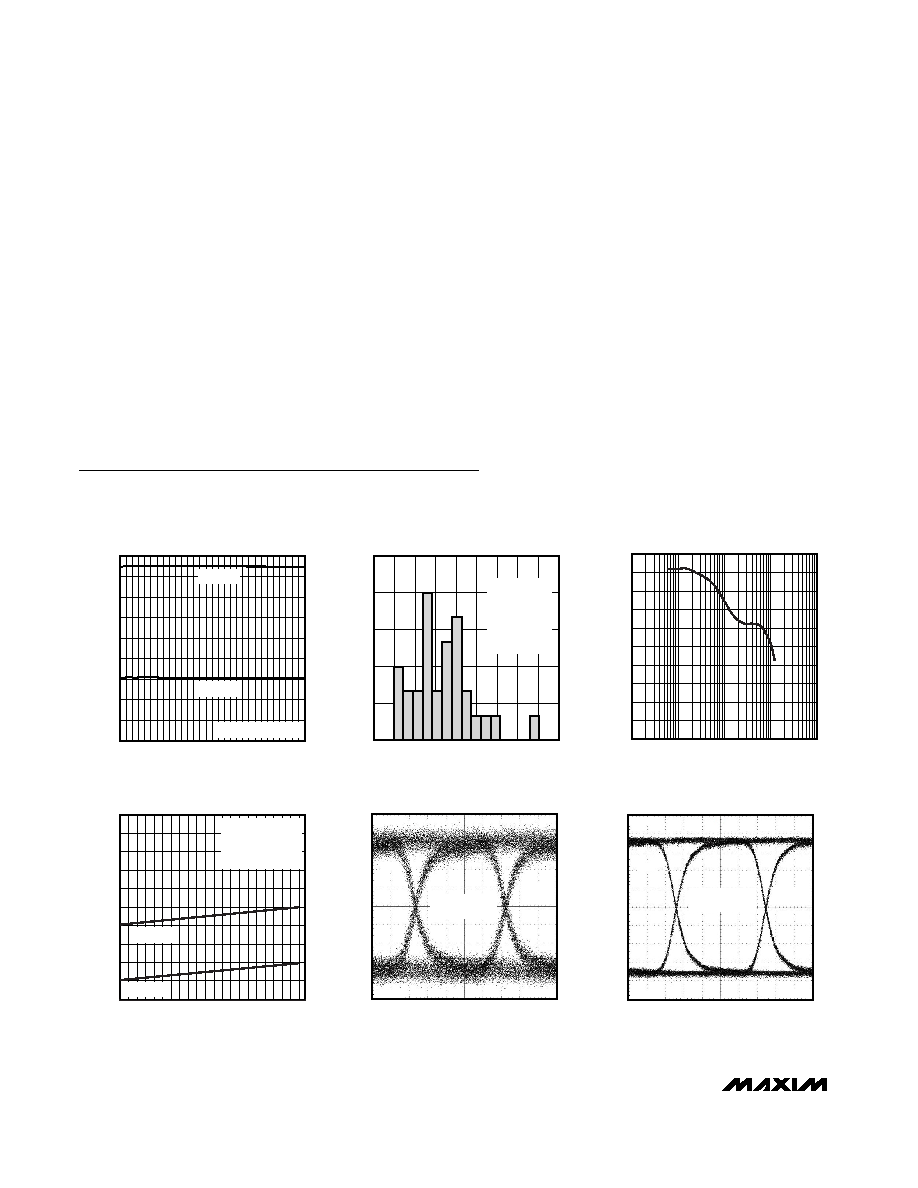
Typical Operating Characteristics
(VCC = +3.3V, TA = +25°C, unless otherwise noted.)
100
300
200
600
500
400
900
800
700
1000
0
400
200
600
800
1000
1200
OUTPUT AMPLITUDE
vs. INPUT AMPLITUDE
MAX3861
toc01
INPUT AMPLITUDE (mVP-P)
OUTPUT
AMPLITUDE
(mV
P-P
)
VSC = 2.0V
VSC = GND
223 - 1PRBS AT 2.7Gbps
DISTRIBUTION OF SD HYSTERESIS
(WORST-CASE CONDITIONS)
MAX3861
toc02
SD HYSTERESIS (dB)
PERCENT
OF
UNITS
(%)
7.0
6.5
6.0
5.5
5.0
4.5
4.0
3.5
5
10
15
20
25
0
3.0
7.5
VCC = 3.0V
VSC = 2.0V
VIN = 2mVP-P
TA = -40°C
MEAN = 4.52dB
σ = 0.79dB
DETERMINISTIC JITTER
vs. INPUT AMPLITUDE
MAX3861
toc03
INPUT AMPLITUDE (mVP-P)
DETERMINISTIC
JITTER
(ps
P-P
)
1000
100
10
2
4
6
8
10
12
14
16
18
20
0
1
10,000
50
65
60
55
70
75
80
85
90
95
100
-40
-10
20
50
80
SUPPLY CURRENT vs. TEMPERATURE
MAX3861
toc04
TEMPERATURE (°C)
SUPPLY
CURRENT
(mA)
EN = VCC
EN = GND
EXCLUDES OUTPUT
LOAD CURRENTS
VIN = 1200mVP-P
VSC = 0
76ps/div
EYE DIAGRAM, MINIMUM INPUT
MAX3861
toc05
VIN = 6mVP-P
223 - 1PRBS
76ps/div
MAX3861
toc06
VIN = 1200mVP-P
223 - 1PRBS
EYE DIAGRAM, MAXIMUM INPUT
Note 5:
See the Distribution of Differential Output Offset (Worst-Case Conditions) graph in the Typical Operating Characteristics.
Note 6:
Characterized with a 675Mbps 1-0 pattern.
Note 7:
Measurements are taken over an input signal range of 16dB.
Note 8:
Deterministic jitter is defined as the arithmetic sum of PWD (pulse-width distortion) and PDJ (pattern-dependent jitter).
Deterministic jitter is the difference between total jitter and random jitter, with system jitter calibrated out. It is measured
with a 27 - 1PRBS, and 80CIDs with DC-coupled outputs.
Note 9:
The typical input resistance of the SC pin is 40k.
Note 10: AGC loop time constant is measured with a 20dB change in the input and VSC held constant. With an external capacitor
CCG of 0.022F connected between CG+ and CG-, a typical AGC loop time constant of 760s is achieved.
Note 11: SD deassert time depends on the AGC loop time constant set by CCG.
Note 12: SD accuracy is defined as the part-to-part variation of the SD threshold at a fixed RTH value.
Note 13: See the Distribution of SD Hysteresis (Worst-Case Conditions) graph in the Typical Operating Characteristics.
Note 14: Measurements are taken over an input signal range of 20dB.
ELECTRICAL CHARACTERISTICS (continued)
(VCC = +3.0V to +3.6V, TA = -40°C to +85°C. Typical values are at VCC = +3.3V and TA = +25°C, unless otherwise noted.) (Note 1)
相关PDF资料 |
PDF描述 |
|---|---|
| MAX3945ETE+ | IC AMP LIMITING 3.3V LP 16TQFN |
| MAX3964AETP+T | IC AMP LIMITING SGNL DET 20-TQFN |
| MAX3969ETP+T | IC AMP LIMIT 200MBPS 20-TQFN |
| MAX3971AUTP+T | IC AMP LIMIT 10.7GBPS 20-TQFN |
| MAX4025EUP+ | IC AMP VIDEO MUX 2:1 20-TSSOP |
相关代理商/技术参数 |
参数描述 |
|---|---|
| MAX3861EGG-T | 功能描述:限幅放大器 2.7Gbps Post Amp w/Auto Gain Control RoHS:否 制造商:Micrel 输入电压范围(最大值):3.6 V 工作电源电压:3.3 V 电源电流:40 mA 工作温度范围:- 40 C to + 85 C 封装 / 箱体:MSOP-10 封装:Tube |
| MAX3861ETG+ | 功能描述:限幅放大器 2.7Gbps Post Amp w/Auto Gain Control RoHS:否 制造商:Micrel 输入电压范围(最大值):3.6 V 工作电源电压:3.3 V 电源电流:40 mA 工作温度范围:- 40 C to + 85 C 封装 / 箱体:MSOP-10 封装:Tube |
| MAX3861ETG+T | 功能描述:限幅放大器 2.7Gbps Post Amp w/Auto Gain Control RoHS:否 制造商:Micrel 输入电压范围(最大值):3.6 V 工作电源电压:3.3 V 电源电流:40 mA 工作温度范围:- 40 C to + 85 C 封装 / 箱体:MSOP-10 封装:Tube |
| MAX3861EVKIT | 功能描述:放大器 IC 开发工具 RoHS:否 制造商:International Rectifier 产品:Demonstration Boards 类型:Power Amplifiers 工具用于评估:IR4302 工作电源电压:13 V to 23 V |
| MAX3863E/D | 功能描述:激光驱动器 RoHS:否 制造商:Micrel 数据速率:4.25 Gbps 工作电源电压:3 V to 3.6 V 电源电流:80 mA 最大工作温度:+ 85 C 封装 / 箱体:QFN-16 封装:Tube |
发布紧急采购,3分钟左右您将得到回复。