- 您现在的位置:买卖IC网 > PDF目录8600 > MAX3861ETG+T (Maxim Integrated Products)IC AMP POST W/AGC 24-TQFN-EP PDF资料下载
参数资料
| 型号: | MAX3861ETG+T |
| 厂商: | Maxim Integrated Products |
| 文件页数: | 10/13页 |
| 文件大小: | 0K |
| 描述: | IC AMP POST W/AGC 24-TQFN-EP |
| 产品培训模块: | Lead (SnPb) Finish for COTS Obsolescence Mitigation Program |
| 标准包装: | 2,500 |
| 类型: | 后置放大器 |
| 应用: | 光纤学网络 |
| 安装类型: | 表面贴装 |
| 封装/外壳: | 24-WFQFN 裸露焊盘 |
| 供应商设备封装: | 24-TQFN-EP(4x4) |
| 包装: | 带卷 (TR) |
MAX3861
2.7Gbps Post Amp with Automatic Gain Control
6
_______________________________________________________________________________________
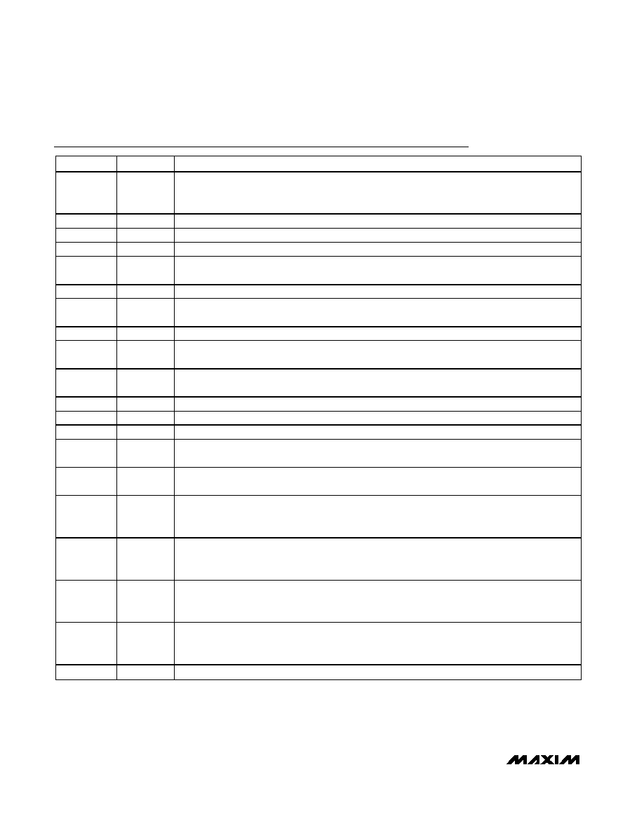
Pin Description
PIN
NAME
FUNCTION
1TH
Input Signal Detect Threshold Programming Pin. Attach a resistor between this pin and ground to
program the input signal detect assert threshold. Leaving this pin open sets the signal detect
threshold to its absolute minimum value (<2mVP-P). See the Design Procedure section.
2, 5, 14, 17
VCC
Supply Voltage Connection. Connect all VCC pins to the board VCC plane.
3
IN+
Positive CML Signal Input with On-Chip Termination Resistor
4
IN-
Negative CML Signal Input with On-Chip Termination Resistor
6EN
Signal Detect Enable. Set high (
≥2.0V) or leave open to enable the input signal detection (RSSI and
SD) circuitry. Set low (
≤0.4V) to power down the input signal detection circuitry.
7VREF
Reference Voltage Output (2.0V). Connect this pin to the SC pin for maximum output signal swing.
8SC
Output Amplitude External Control. Ground SC for minimum output amplitude. Apply 2.0V to SC or
connect SC directly to VREF for maximum output amplitude.
9, 12, 22
GND
Ground. Connect all GND pins to the board ground plane.
10
CG+
Connection for AGC Loop Capacitor. A capacitor connected between CG+ and CG- sets the AGC
loop time constant.
11
CG-
Connection for AGC Loop Capacitor. A capacitor connected between CG+ and CG- sets the AGC
loop time constant.
13
OSM
Output Signal Monitor. This DC signal is linearly proportional to the output signal amplitude.
15
OUT-
Negative CML Data Output with On-Chip Back-Termination Resistor
16
OUT+
Positive CML Data Output with On-Chip Back-Termination Resistor
18
SD
Input Signal Detect. Asserts logic low when the input signal level drops below the programmed
threshold.
19
RSSI
Received Signal Strength Indicator. Outputs a DC signal linearly proportional to the input signal
amplitude.
20
CD-
Connection for Signal Detect Capacitor. A capacitor connected between CD+ and CD- sets the
offset-cancellation loop time constant of the input signal detection. See the Detailed Description
section.
21
CD+
Connection for Signal Detect Capacitor. A capacitor connected between CD+ and CD- sets the
offset-cancellation loop time constant of the input signal detection. See the Detailed Description
section.
23
CZ-
Connection for Offset-Cancellation Loop Capacitor. A capacitor connected between CZ+ and CZ-
sets the offset-cancellation loop time constant of the main signal path. See the Detailed Description
section.
24
CZ+
Connection for Offset-Cancellation Loop Capacitor. A capacitor connected between CZ+ and CZ-
sets the offset-cancellation loop time constant of the main signal path. See the Detailed Description
section.
EP
Exposed Pad
Maxim recommends connecting the exposed pad to board ground.
相关PDF资料 |
PDF描述 |
|---|---|
| VE-2TV-IV-F3 | CONVERTER MOD DC/DC 5.8V 150W |
| MAX9000ESA+ | IC OP AMP LP HI SPEED 8-SOIC |
| VE-2TV-IV-F2 | CONVERTER MOD DC/DC 5.8V 150W |
| VI-252-IV-F1 | CONVERTER MOD DC/DC 15V 150W |
| VI-24V-IV-F4 | CONVERTER MOD DC/DC 5.8V 150W |
相关代理商/技术参数 |
参数描述 |
|---|---|
| MAX3861EVKIT | 功能描述:放大器 IC 开发工具 RoHS:否 制造商:International Rectifier 产品:Demonstration Boards 类型:Power Amplifiers 工具用于评估:IR4302 工作电源电压:13 V to 23 V |
| MAX3863E/D | 功能描述:激光驱动器 RoHS:否 制造商:Micrel 数据速率:4.25 Gbps 工作电源电压:3 V to 3.6 V 电源电流:80 mA 最大工作温度:+ 85 C 封装 / 箱体:QFN-16 封装:Tube |
| MAX3863EGJ | 功能描述:激光驱动器 2.7Gbps Laser Driver w/Modulation Comp RoHS:否 制造商:Micrel 数据速率:4.25 Gbps 工作电源电压:3 V to 3.6 V 电源电流:80 mA 最大工作温度:+ 85 C 封装 / 箱体:QFN-16 封装:Tube |
| MAX3863EGJ-T | 功能描述:激光驱动器 2.7Gbps Laser Driver w/Modulation Comp RoHS:否 制造商:Micrel 数据速率:4.25 Gbps 工作电源电压:3 V to 3.6 V 电源电流:80 mA 最大工作温度:+ 85 C 封装 / 箱体:QFN-16 封装:Tube |
| MAX3863ETJ+ | 功能描述:激光驱动器 2.7Gbps Laser Driver w/Modulation Comp RoHS:否 制造商:Micrel 数据速率:4.25 Gbps 工作电源电压:3 V to 3.6 V 电源电流:80 mA 最大工作温度:+ 85 C 封装 / 箱体:QFN-16 封装:Tube |
发布紧急采购,3分钟左右您将得到回复。