- 您现在的位置:买卖IC网 > PDF目录11699 > MAX3885ECB+D (Maxim Integrated Products)IC 1:16 DESERIALIZER 64-TQFP PDF资料下载
参数资料
| 型号: | MAX3885ECB+D |
| 厂商: | Maxim Integrated Products |
| 文件页数: | 5/8页 |
| 文件大小: | 0K |
| 描述: | IC 1:16 DESERIALIZER 64-TQFP |
| 产品培训模块: | Lead (SnPb) Finish for COTS Obsolescence Mitigation Program |
| 标准包装: | 160 |
| 功能: | 解串器 |
| 数据速率: | 2.5Gbps |
| 输入类型: | PECL |
| 输出类型: | LVDS |
| 输入数: | 1 |
| 输出数: | 16 |
| 电源电压: | 3 V ~ 3.6 V |
| 工作温度: | -40°C ~ 85°C |
| 安装类型: | 表面贴装 |
| 封装/外壳: | 64-LQFP |
| 供应商设备封装: | 64-LQFP(10x10) |
| 包装: | 托盘 |
MAX3885
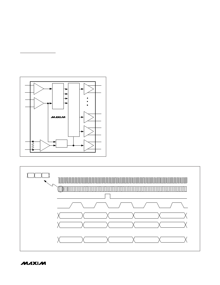
Detailed Description
The MAX3885 deserializer uses a 16-bit shift register,
16-bit parallel output register, 4-bit counter, PECL input
buffers, and low-voltage differential-signal (LVDS)
input/output buffers to convert 2.488Gbps serial data to
16-bit wide, 155Mbps parallel data (Figure 2). The input
shift register continuously clocks incoming data on the
positive transition of the serial clock (SCLK) input sig-
nal. The 4-bit counter generates a parallel-output clock
(PCLK) by dividing the serial-clock frequency by 16.
The PCLK signal clocks the parallel-output register.
During normal operation, the counter divides the SCLK
frequency by 16, causing the output register to latch
every 16 bits of incoming serial data. The synchroniza-
tion inputs (SYNC+, SYNC-) realign and reframe data.
When the SYNC signal is pulsed high for at least four
SCLK cycles, the parallel output data is delayed by one
SCLK cycle. This realignment is guaranteed to occur
within two complete PCLK cycles of the SYNC signal’s
positive transition. As a result, the first incoming bit of
data during that PCLK cycle is dropped, shifting the
alignment between PCLK and data by one bit. See
Figure 3 for the timing diagram and Figure 4 for the tim-
ing parameters diagram.
Low-Voltage Differential-Signal (LVDS)
Inputs and Outputs
The MAX3885 features LVDS inputs and outputs for
interfacing with high-speed digital circuitry. The LVDS
standard is based on the IEEE 1596.3 LVDS specifica-
tion. This technology uses 500mVp-p to 800mVp-p dif-
ferential low-voltage swings to achieve fast transition
times, minimize power dissipation, and improve noise
immunity. The parallel clock and data LVDS outputs
(PCLK+, PCLK-, PD_+, PD_-) require 100
Ω differential
+3.3V, 2.488Gbps, SDH/SONET
1:16 Deserializer with LVDS Outputs
_______________________________________________________________________________________
5
16-BIT
SHIFT
REGISTER
16-BIT
PARALLEL
OUTPUT
REGISTER
4-BIT
COUNTER
LVDS
PECL
LVDS
PD15+
PD15-
PD1+
PD1-
PD0+
PD0-
PCLK+
PCLK-
SD+
SD-
SCLK+
SCLK-
SYNC+
SYNC-
100
Ω
MAX3885
Figure 2. Functional Diagram
SCLK
SD
SYNC
PCLK
D0
D15
D14
D13
D16
D32
D48
ONE BIT HAS SLIPPED
IN THIS TIME SLICE
D65
(LSB) PD0
D1
D17
D33
D49
D66
PD1
D15
(MSB)
TRANSMITTED FIRST
D31
D47
D64
D80
PD15
Figure 3. Timing Diagram
相关PDF资料 |
PDF描述 |
|---|---|
| C8051F575-IM | IC 8051 MCU 16K FLASH 40-QFN |
| R5F1008CALA#U0 | MCU 16BIT 32KB FLASH 25FLGA |
| R5F100CAALA#U0 | MCU 16BIT 16KB FLASH 36FLGA |
| R5F1007DANA#U0 | MCU 16BIT 48KB FLASH 24WQFN |
| P87C52X2BA,512 | IC 80C51 MCU 8K OTP 44-PLCC |
相关代理商/技术参数 |
参数描述 |
|---|---|
| MAX3885ECB-TD | 功能描述:串行器/解串器 - Serdes 3.3V 2.488Gbps SDH/ SONET 1:16 Deserial RoHS:否 制造商:Texas Instruments 类型:Deserializer 数据速率:1.485 Gbit/s 输入类型:ECL/LVDS 输出类型:LVCMOS 输入端数量:1 输出端数量:20 工作电源电压:2.375 V to 2.625 V 工作温度范围:0 C to + 70 C 封装 / 箱体:TQFP-64 |
| MAX3885EVKIT | 功能描述:串行器/解串器 - Serdes Evaluation Kit for the MAX3885 RoHS:否 制造商:Texas Instruments 类型:Deserializer 数据速率:1.485 Gbit/s 输入类型:ECL/LVDS 输出类型:LVCMOS 输入端数量:1 输出端数量:20 工作电源电压:2.375 V to 2.625 V 工作温度范围:0 C to + 70 C 封装 / 箱体:TQFP-64 |
| MAX3886ETN+ | 功能描述:串行器/解串器 - Serdes CDR w/Integrated Serial/Deserializer RoHS:否 制造商:Texas Instruments 类型:Deserializer 数据速率:1.485 Gbit/s 输入类型:ECL/LVDS 输出类型:LVCMOS 输入端数量:1 输出端数量:20 工作电源电压:2.375 V to 2.625 V 工作温度范围:0 C to + 70 C 封装 / 箱体:TQFP-64 |
| MAX3886ETN+T | 功能描述:串行器/解串器 - Serdes CDR w/Integrated Serial/Deserializer RoHS:否 制造商:Texas Instruments 类型:Deserializer 数据速率:1.485 Gbit/s 输入类型:ECL/LVDS 输出类型:LVCMOS 输入端数量:1 输出端数量:20 工作电源电压:2.375 V to 2.625 V 工作温度范围:0 C to + 70 C 封装 / 箱体:TQFP-64 |
| MAX388C/D | 功能描述:多路器开关 IC RoHS:否 制造商:Texas Instruments 通道数量:1 开关数量:4 开启电阻(最大值):7 Ohms 开启时间(最大值): 关闭时间(最大值): 传播延迟时间:0.25 ns 工作电源电压:2.3 V to 3.6 V 工作电源电流: 最大工作温度:+ 85 C 安装风格:SMD/SMT 封装 / 箱体:UQFN-16 |
发布紧急采购,3分钟左右您将得到回复。