- 您现在的位置:买卖IC网 > PDF目录11697 > MAX3892ETH+ (Maxim Integrated Products)IC 4:1 SERIALIZER SONET 44-TQFN PDF资料下载
参数资料
| 型号: | MAX3892ETH+ |
| 厂商: | Maxim Integrated Products |
| 文件页数: | 8/11页 |
| 文件大小: | 0K |
| 描述: | IC 4:1 SERIALIZER SONET 44-TQFN |
| 产品培训模块: | Lead (SnPb) Finish for COTS Obsolescence Mitigation Program |
| 标准包装: | 43 |
| 功能: | 串行器 |
| 数据速率: | 2.7Gbps |
| 输入类型: | LVDS |
| 输出类型: | CML |
| 输入数: | 4 |
| 输出数: | 1 |
| 电源电压: | 3 V ~ 3.6 V |
| 工作温度: | -40°C ~ 85°C |
| 安装类型: | 表面贴装 |
| 封装/外壳: | 44-WFQFN 裸露焊盘 |
| 供应商设备封装: | 44-TQFN-EP(7x7) |
| 包装: | 管件 |
MAX3892
+3.3V, 2.5Gbps/2.7Gbps, SDH/SONET 4:1
Serializer with Clock Synthesis
6
_______________________________________________________________________________________
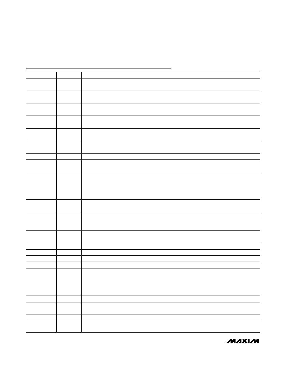
Pin Description (continued)
PIN
NAME
FUNCTION
9
SLBO-
Negative System Loop-Back Output or 622MHz/666MHz Clock Output. Select CML data or clock
as shown in Table 1.
10
SLBO+
Positive System Loop-Back Output or 622MHz/666MHz Clock Output. Select CML data or clock as
shown in Table 1.
12
SLBPD
System Loopback Power Down, TTL Input. SLPD = high activates the system loopback output
driver; SLBPD = low powers down the loop-back output driver.
13
SLBEN
System Loop-Back Enable Input, TTL Input. SLBEN = high activates the system loop-back output;
SLBEN = low activates the 622MHz/666MHz reference clock output.
14
RESET
FIFO Reset, TTL Input. An active-high reset recenters the FIFO to tolerate maximum skew between
PCLKI and PCLKO.
15
FIFOERROR
FIFO Error Indicator, TTL Output. Active high when the read/write clocks access the same FIFO
address. This signal may be used to control RESET.
17, 28, 36, 43
VCC
Supply Voltage, +3.3V
18
LOL
Loss of Lock, TTL Output. An active low indicates that the VCO and reference frequency differ by
500ppm.
19
MODE
Clock Control Input:
MODE = GND; fPCLKI = 311.04MHz/333MHz with SCLKO active
MODE = 30k
Ω to GND; fPCLKI = 311.04MHz/333MHz with SCLKO off
MODE = OPEN (float); fPCLKI = 622.08MHz/666MHz with SCLKO off
MODE = VCC; fPCLKI = 622.08MHz/666MHz with SCLKO active
20
PCLKI+
Positive Parallel Clock, LVDS Input. Data is written to the input register on the clock rising edge in
622Mbps mode and on both rising and falling edges in 311Mbps mode (Figure 1).
21
PCLKI-
Negative Parallel Clock, LVDS Input (Figure 1).
23, 25, 29, 31
PDI3+ to
PDI0+
Positive Data Inputs, LVDS (622Mbps or 666Mbps)
24, 26, 30, 32
PDI3- to
PDI0-
Negative Data Inputs, LVDS (622Mbps or 666Mbps)
34
PCLKO+
Positive Parallel Clock Output, LVDS. This clock may be 622.08MHz or 666MHz.
35
PCLKO-
Negative Parallel Clock Output, LVDS. This clock may be 622.08MHz or 666MHz.
37
RCLK+
Positive Reference Clock Input, LVPECL
38
RCLK-
Negative Reference Clock Input, LVPECL
39
CLKSET
Reference Clock Rate Programming Pin:
CLKSET = VCC; RCLK = 622.08MHz/666MHz
CLKSET = OPEN (float); RCLK = 155.52MHz/167MHz
CLKSET = 30k
Ω to GND; RCLK = 77.76MHz/83.3MHz
CLKSET = GND; RCLK = 38.88MHz/41.6MHz
40
RATESET
Data Rate Select, TTL Input. RATESET = high for 2.666Gbps, RATESET = low for 2.488Gbps.
41
VCCVCO
Supply Voltage for VCO +3.3V. Add bypass capacitors near this pin before connecting to the VCC
power plane.
42
FIL
PLL Capacitor Pin. Connect a 0.1F capacitor from this pin to VCCVCO.
EP
Exposed
Paddle
The exposed paddle must be soldered to ground for proper thermal and electrical operation.
相关PDF资料 |
PDF描述 |
|---|---|
| V72C24H150BL3 | CONVERTER MOD DC/DC 24V 150W |
| MAX3681EAG+ | IC 1:4 DESERIALIZR W/LVDS 24SSOP |
| MAX9217ETM+ | IC SERIALIZER LVDS 48-TQFN |
| MAX9242EUM+ | SEMICONDUCTOR OTHER |
| MAX3680EAI+ | IC DESERIALZR 622MBPS TTL 28SSOP |
相关代理商/技术参数 |
参数描述 |
|---|---|
| MAX3892ETH+ | 功能描述:串行器/解串器 - Serdes 3.3V 2.5/2.7Gbps SDH /SONET 4:1 Serial RoHS:否 制造商:Texas Instruments 类型:Deserializer 数据速率:1.485 Gbit/s 输入类型:ECL/LVDS 输出类型:LVCMOS 输入端数量:1 输出端数量:20 工作电源电压:2.375 V to 2.625 V 工作温度范围:0 C to + 70 C 封装 / 箱体:TQFP-64 |
| MAX3892ETH+D | 制造商:Maxim Integrated Products 功能描述:3.3V 2.5GBPS/2.7GBPS SDH/SONET 4: - Rail/Tube |
| MAX3892ETH+T | 功能描述:串行器/解串器 - Serdes 3.3V 2.5/2.7Gbps SDH /SONET 4:1 Serial RoHS:否 制造商:Texas Instruments 类型:Deserializer 数据速率:1.485 Gbit/s 输入类型:ECL/LVDS 输出类型:LVCMOS 输入端数量:1 输出端数量:20 工作电源电压:2.375 V to 2.625 V 工作温度范围:0 C to + 70 C 封装 / 箱体:TQFP-64 |
| MAX3892ETH+TD | 制造商:Maxim Integrated Products 功能描述:3.3V 2.5GBPS/2.7GBPS SDH/SONET 4: - Tape and Reel |
| MAX389C/D | 功能描述:多路器开关 IC RoHS:否 制造商:Texas Instruments 通道数量:1 开关数量:4 开启电阻(最大值):7 Ohms 开启时间(最大值): 关闭时间(最大值): 传播延迟时间:0.25 ns 工作电源电压:2.3 V to 3.6 V 工作电源电流: 最大工作温度:+ 85 C 安装风格:SMD/SMT 封装 / 箱体:UQFN-16 |
发布紧急采购,3分钟左右您将得到回复。