- 您现在的位置:买卖IC网 > PDF目录9766 > MAX3984UTE+T (Maxim Integrated Products)IC PREMP DRIVER 1CH 16-TQFN PDF资料下载
参数资料
| 型号: | MAX3984UTE+T |
| 厂商: | Maxim Integrated Products |
| 文件页数: | 14/18页 |
| 文件大小: | 0K |
| 描述: | IC PREMP DRIVER 1CH 16-TQFN |
| 产品培训模块: | Lead (SnPb) Finish for COTS Obsolescence Mitigation Program |
| 标准包装: | 2,500 |
| 类型: | 驱动器 |
| 驱动器/接收器数: | 1/0 |
| 规程: | 以太网 |
| 电源电压: | 3 V ~ 3.6 V |
| 安装类型: | 表面贴装 |
| 封装/外壳: | 16-WFQFN 裸露焊盘 |
| 供应商设备封装: | 16-TQFN-EP(3x3) |
| 包装: | 带卷 (TR) |
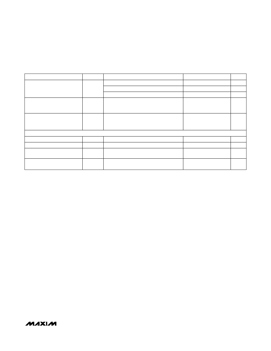
PARAMETER
SYMBOL
CONDITIONS
MIN
TYP
MAX
UNITS
LOS asserted
0
25
μA
LOS asserted; VOL
0.4V
1.0
mA
LOS Open-Collector Current
Sink
(Note 12)
0
25
μA
LOS Response Time
(Note 4)
Time from VIN dropping below deassert level
or rising above assert level to 50% point of
LOS output transition
10
μs
LOS Transition Time
Rise time or fall time (10% to 90%);
pullup supply = 5.5V; external pullup
R
4.7k
200
ns
CONTROL INPUTS: TX_DISABLE, PE0, PE1, OUT_LEV, IN_LEV
Logic-High Voltage
VIH
2.0
V
Logic-Low Voltage
VIL
0.8
V
Logic-High Current
IIH
Current required to maintain logic-high state
at VIH > +2.0V
-150
μA
Logic-Low Current
IIL
Current required to maintain logic-low state
at VIL < +0.8V
350
μA
MAX3984
1Gbps to 10Gbps Preemphasis Driver with
Receive Equalizer
_______________________________________________________________________________________
5
Note 1:
Supply voltage to reach 90% of final value in less than 100s, but not less than 10s. Power-on delay interval measured
from the 50% level of the final voltage at the filter’s device side to 50% level of final current. The supply is to remain at or
above 3V for at least 100ms. Only one full-scale transition is permitted during this interval. Aberrations on the transition are
limited to less than 100mV.
Note 2:
IN+ and IN- are single-ended, 50
Ω terminations to (VCC - 1.5V) ±0.2V.
Note 3:
Load is 50
Ω ±1% at each side and the pattern is 0000011111 or equivalent pattern at 2.5Gbps.
Note 4:
Guaranteed by design and characterization.
Note 5:
PE1 = PE0 = logic-high (maximum preemphasis), load is 50
Ω ±1% at each side. The pattern is 11001100 (50% edge den-
sity) at 10Gbps. AC common-mode output is computed as:
VACCM_RMS = RMS[(VP + VN) / 2) - VDCCM]
where:
VP = time-domain voltage measured at OUT+ with at least 10GHz bandwidth.
VN = time-domain voltage measured at OUT- with at least 10GHz bandwidth.
AC common-mode voltage (VACCM_RMS) expressed as an RMS value.
DC common-mode voltage (VDCCM) = average DC voltage of (VP + VN) / 2.
Note 6:
Using 0000011111 or equivalent pattern at 2.5Gbps. PE0 = PE1 = logic-low for minimum preemphasis. Measured within
2in of the output pins with Rogers 4350 dielectric, or equivalent, and
≥ 10-mil line width. For transition time, the 0% refer-
ence is the steady state level after four zeros, just before the transition, and the 100% reference level is the steady state
level after four consecutive logic ones.
Note 7:
Pattern is 0000011111 or equivalent pattern at 10Gbps and 100mVP-P differential swing. IN_LEV = logic-low and PE0 =
PE1 = logic-low for minimum preemphasis. Signal transition time is controlled by the 4th-order BT filter (7.5GHz band-
width) or equivalent. See Figure 3 for setup.
Note 8:
Test pattern (464 bits): 100 zeros, 1010, PRBS7, 100 ones, 0101, PRBS7.
Note 9:
Input range selection is IN_LEV = logic-high for FR-4 input equalization. Cables are unequalized, Amphenol Spectra-Strip
(160-2499-997) 24 AWG or equivalent. Residual deterministic jitter is the difference between the source jitter at point A
and the load jitter point D in Figure 2. The deterministic jitter (DJ) at the output of the transmission line must be from media
induced loss and not from clock source modulation. DJ is measured at point D of Figure 2.
Note 10: Input range selection is IN_LEV = logic-low. Residual deterministic jitter is the difference between the source jitter at point
A and the load jitter point D in Figure 3. The deterministic jitter (DJ) at the output of the transmission line must be from
media induced loss and not from clock source modulation. DJ is measured at point D of Figure 3.
Note 11: Measured with 101010… pattern at 10Gbps with less than 1in of FR-4 at the input.
Note 12: True open-collector outputs. VCC = 0 and the external 4.7k
Ω pullup resistor is connected to +5.5V.
ELECTRICAL CHARACTERISTICS (continued)
(VCC = +3.0V to +3.6V, TA = 0°C to +85°C. Typical values are at TA = +25°C, VCC = +3.3V, unless otherwise noted.)
相关PDF资料 |
PDF描述 |
|---|---|
| MAX3130EAI+T | IC TXRX W/RS232 28-SSOP |
| IDT74SSTUAE32866ABFG8 | IC BUFFER 25BIT CONF REG 96-BGA |
| MS27473T18B35PB | CONN PLUG 66POS STRAIGHT W/PINS |
| D38999/20WG16SB | CONN RCPT 16POS WALL MNT W/SCKT |
| MS27484T16B26P | CONN PLUG 26POS STRAIGHT W/PINS |
相关代理商/技术参数 |
参数描述 |
|---|---|
| MAX3986EVKIT+ | 制造商:Maxim Integrated Products 功能描述:EVAL KIT MAX3986 (1GBPS TO 10.3GBPS LINEAR EQUALIZER) - Boxed Product (Development Kits) |
| MAX3986UTU+ | 功能描述:IC EQUALIZER LOW PWR 4CH 38TQFN RoHS:是 类别:集成电路 (IC) >> 接口 - 专用 系列:- 标准包装:3,000 系列:- 应用:PDA,便携式音频/视频,智能电话 接口:I²C,2 线串口 电源电压:1.65 V ~ 3.6 V 封装/外壳:24-WQFN 裸露焊盘 供应商设备封装:24-QFN 裸露焊盘(4x4) 包装:带卷 (TR) 安装类型:表面贴装 产品目录页面:1015 (CN2011-ZH PDF) 其它名称:296-25223-2 |
| MAX3986UTU+T | 功能描述:IC EQUALIZER LOW PWR 4CH 38TQFN RoHS:是 类别:集成电路 (IC) >> 接口 - 专用 系列:- 标准包装:3,000 系列:- 应用:PDA,便携式音频/视频,智能电话 接口:I²C,2 线串口 电源电压:1.65 V ~ 3.6 V 封装/外壳:24-WQFN 裸露焊盘 供应商设备封装:24-QFN 裸露焊盘(4x4) 包装:带卷 (TR) 安装类型:表面贴装 产品目录页面:1015 (CN2011-ZH PDF) 其它名称:296-25223-2 |
| MAX3987ETM+ | 功能描述:IC EQUALIZER/DRIVER QUAD 48TQFN RoHS:是 类别:集成电路 (IC) >> 接口 - 专用 系列:- 标准包装:3,000 系列:- 应用:PDA,便携式音频/视频,智能电话 接口:I²C,2 线串口 电源电压:1.65 V ~ 3.6 V 封装/外壳:24-WQFN 裸露焊盘 供应商设备封装:24-QFN 裸露焊盘(4x4) 包装:带卷 (TR) 安装类型:表面贴装 产品目录页面:1015 (CN2011-ZH PDF) 其它名称:296-25223-2 |
| MAX3987ETM+T | 功能描述:IC EQUALIZER/DRIVER QUAD 48TQFN RoHS:是 类别:集成电路 (IC) >> 接口 - 专用 系列:- 标准包装:3,000 系列:- 应用:PDA,便携式音频/视频,智能电话 接口:I²C,2 线串口 电源电压:1.65 V ~ 3.6 V 封装/外壳:24-WQFN 裸露焊盘 供应商设备封装:24-QFN 裸露焊盘(4x4) 包装:带卷 (TR) 安装类型:表面贴装 产品目录页面:1015 (CN2011-ZH PDF) 其它名称:296-25223-2 |
发布紧急采购,3分钟左右您将得到回复。