- 您现在的位置:买卖IC网 > PDF目录2009 > MAX3991UTG+T (Maxim Integrated Products)IC DATA RECOVERY W/AMP 24-TQFN PDF资料下载
参数资料
| 型号: | MAX3991UTG+T |
| 厂商: | Maxim Integrated Products |
| 文件页数: | 11/12页 |
| 文件大小: | 0K |
| 描述: | IC DATA RECOVERY W/AMP 24-TQFN |
| 标准包装: | 2,500 |
| 类型: | 时钟和数据恢复(CDR) |
| PLL: | 是 |
| 主要目的: | SONET/SDH.XFP 光学接收器 |
| 输入: | CML |
| 输出: | CML |
| 电路数: | 1 |
| 比率 - 输入:输出: | 1:2 |
| 差分 - 输入:输出: | 是/是 |
| 频率 - 最大: | 693.5MHz |
| 电源电压: | 3 V ~ 3.6 V |
| 工作温度: | 0°C ~ 85°C |
| 安装类型: | 表面贴装 |
| 封装/外壳: | 24-WFQFN 裸露焊盘 |
| 供应商设备封装: | 24-TQFN-EP(4x4) |
| 包装: | 带卷 (TR) |
MAX3991
Detailed Description
The MAX3991 clock and data recovery with limiting
amplifier restores data to XFI specifications. It consists of
a limiting amplifier with LOS power detector, and a PLL
data retimer with LOL indicator. An optional recovered
clock may also be enabled for performance testing.
Limiting Amplifier
The SDI inputs of the MAX3991 accept serial NRZ data
from the optical receiver assembly. The limiting amplifier
accepts signals as small as 7mVP-P and amplifies them
to allow recovery by the CDR. The limiting amplifier uses
an offset cancellation circuit to compensate for device
mismatch within the gain stages. The low-frequency cut-
off of the offset cancellation loop is typically 30kHz.
10Gbps Clock and Data Recovery
with Limiting Amplifier
8
_______________________________________________________________________________________
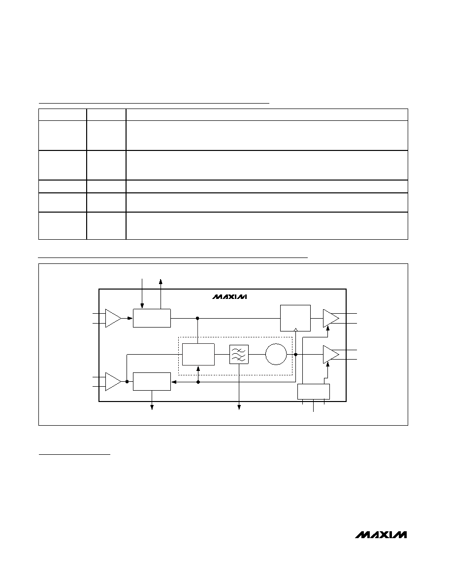
Figure 3. Functional Diagram
Functional Diagram
MAX3991
VTH
LIMITING
AMPLIFIER
VCO
DFF
DQ
CML
PHASE/
FREQUENCY
DETECTOR
LOL
DETECTOR
LOS
LOL
FUNCTIONAL
CONTROL
CFIL
CML
SDI+
SDI-
REFCLK+
REFCLK-
SDO+
SDO-
SCLKO+
SCLKO-
FCTL1
FCTL2
PLL
200
POL
Pin Description (continued)
PIN
NAME
FUNCTION
21
REFCLK+
Positive Reference Clock Input, Digital. The REFCLK inputs are designed to be AC-coupled to the
reference clock source. REFCLK± have a 200
differential impedance. See the Detailed Description
section for more information. See Table 2.
22
REFCLK-
Negative Reference Clock Input, Digital. The REFCLK inputs are designed to be AC-coupled to the
reference clock source. REFCLK± have a 200
differential impedance. See the Detailed Description
section for more information. See Table 2.
23
FCTL1
Function Control Input 1, TTL. See Table 3 for more information.
24
VTH
LOS Threshold Input, Analog. A voltage applied to this input sets the LOS assert threshold. The LOS
power detector can be disabled if VTH is connected to VCC, which forces LOS low.
EP
Exposed
Pad
Supply Ground. The exposed pad must be soldered to the circuit-board ground for proper thermal
and electrical performance. The MAX3991 uses exposed-pad variation T2444-4 in the package
outline drawing. See the exposed-pad package.
相关PDF资料 |
PDF描述 |
|---|---|
| MAX3992UTG+T | IC DATA RECOVERY W/EQ 24-TQFN |
| MAX504EPD+ | IC DAC 10BIT 5V LP SER 14-DIP |
| MAX507AENG+ | IC DAC 12BIT W/REF 24-DIP |
| MAX5100AEUP+T | IC DAC 8BIT QUAD R-R 20TSSOP |
| MAX5101BEUE+ | IC DAC 8BIT TRPL R-R 16-TSSOP |
相关代理商/技术参数 |
参数描述 |
|---|---|
| MAX3992UTG+ | 功能描述:计时器和支持产品 10Gbps Clock & Data Recovery RoHS:否 制造商:Micrel 类型:Standard 封装 / 箱体:SOT-23 内部定时器数量:1 电源电压-最大:18 V 电源电压-最小:2.7 V 最大功率耗散: 最大工作温度:+ 85 C 最小工作温度:- 40 C 封装:Reel |
| MAX3992UTG+T | 功能描述:计时器和支持产品 10Gbps Clock & Data Recovery RoHS:否 制造商:Micrel 类型:Standard 封装 / 箱体:SOT-23 内部定时器数量:1 电源电压-最大:18 V 电源电压-最小:2.7 V 最大功率耗散: 最大工作温度:+ 85 C 最小工作温度:- 40 C 封装:Reel |
| MAX3996CGP | 功能描述:激光驱动器 3-5.5V 2.5Gbps VCSEL & Laser Driver RoHS:否 制造商:Micrel 数据速率:4.25 Gbps 工作电源电压:3 V to 3.6 V 电源电流:80 mA 最大工作温度:+ 85 C 封装 / 箱体:QFN-16 封装:Tube |
| MAX3996CGP-T | 功能描述:激光驱动器 3-5.5V 2.5Gbps VCSEL & Laser Driver RoHS:否 制造商:Micrel 数据速率:4.25 Gbps 工作电源电压:3 V to 3.6 V 电源电流:80 mA 最大工作温度:+ 85 C 封装 / 箱体:QFN-16 封装:Tube |
| MAX3996CTP+ | 功能描述:激光驱动器 3-5.5V 2.5Gbps VCSEL & Laser Driver RoHS:否 制造商:Micrel 数据速率:4.25 Gbps 工作电源电压:3 V to 3.6 V 电源电流:80 mA 最大工作温度:+ 85 C 封装 / 箱体:QFN-16 封装:Tube |
发布紧急采购,3分钟左右您将得到回复。