- 您现在的位置:买卖IC网 > PDF目录9528 > MAX3992UTG+ (Maxim Integrated Products)IC DATA RECOVERY W/EQ 24-TQFN PDF资料下载
参数资料
| 型号: | MAX3992UTG+ |
| 厂商: | Maxim Integrated Products |
| 文件页数: | 12/12页 |
| 文件大小: | 0K |
| 描述: | IC DATA RECOVERY W/EQ 24-TQFN |
| 标准包装: | 75 |
| 类型: | 时钟和数据恢复(CDR) |
| PLL: | 是 |
| 主要目的: | SONET/SDH.XFP 光学接收器 |
| 输入: | CML |
| 输出: | CML |
| 电路数: | 1 |
| 比率 - 输入:输出: | 1:2 |
| 差分 - 输入:输出: | 是/是 |
| 频率 - 最大: | 693.5MHz |
| 电源电压: | 3 V ~ 3.6 V |
| 工作温度: | 0°C ~ 85°C |
| 安装类型: | 表面贴装 |
| 封装/外壳: | 24-WFQFN 裸露焊盘 |
| 供应商设备封装: | 24-TQFN-EP(4x4) |
| 包装: | 管件 |
Loss-of-Lock Monitor
The LOL output indicates that the frequency difference
between the recovered clock and the reference clock is
excessive. LOL may assert due to excessive jitter at the
data input, incorrect frequency, or loss of input data.
The LOL detector monitors the frequency difference
between the recovered clock and the reference clock.
The LOL output is asserted high when the frequency
difference exceeds 650ppm.
Loss-of-Signal Monitor
The LOS output indicates a loss of input data. Set VTH
>500mV. When the input signal is removed (<50mV),
LOS will be asserted high.
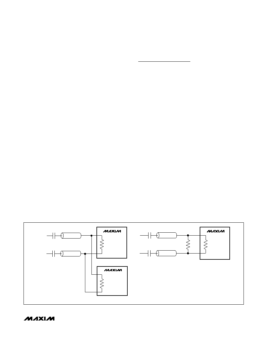
Reference Clock Input
The REFCLK inputs are internally terminated and self-
biased to allow AC-coupling. The input impedance is
100 single-ended (200 differential). The REFCLK
inputs of the MAX3991 and MAX3992 should be con-
nected close together in parallel. The impedance look-
ing into the parallel combination is 100 differential.
This allows both the MAX3991 and MAX3992 to easily
interface with one reference clock without using addi-
tional components. See Figure 4.
Design Procedure
Modes of Operation
The MAX3992 has a standby mode and jitter test mode
in addition to its normal operating mode. Standby is
used to conserve power. In the standby mode, the
power consumption of the MAX3992 falls below 40% of
the normal-operation power consumption. The jitter test
mode enables the SCLK outputs to clock a BERT when
testing jitter generation, jitter transfer, and jitter toler-
ance. The FCTL1 and FCTL2 TTL inputs are used to
select the mode of operation as shown in Table 3.
Serial Data Rate and
Reference Clock Frequency
Input Configuration
The SDI± inputs of the MAX3992 are current-mode
logic (CML) compatible. The inputs have internal 50
terminations for minimum external components. See
Figure 5 for the input structure. For additional informa-
tion on logic interfacing, refer to Maxim Application
Note HFAN 1.0: Introduction to LVDS, PECL, and CML.
Output Configuration
The MAX3992 uses CML for its high-speed digital out-
puts (SDO± and SCLKO±). The configuration of the out-
put circuit includes internal 50 back terminations to
VCC. See Figure 6 for the output structure. CML outputs
may be terminated by 50 to VCC, or by 100 differen-
tial impedance. The relation of the output polarity to input
can be reversed using the POL pin. For additional infor-
mation on logic interfacing, refer to Maxim Application
Note HFAN 1.0: Introduction to LVDS, PECL, and CML.
MAX3992
10Gbps Clock and Data Recovery
with Equalizer
_______________________________________________________________________________________
9
MAX3991
MAX3992
200
50W
REFERENCE
CLOCK
50W
REFERENCE
CLOCK
TRANSCEIVER TERMINATION
TRANSMITTER-ONLY TERMINATION
200
Figure 4. Reference Clock Termination
相关PDF资料 |
PDF描述 |
|---|---|
| VI-B3D-IV-B1 | CONVERTER MOD DC/DC 85V 150W |
| V28A8M200BG | CONVERTER MOD DC/DC 8V 200W |
| DS276S+T&R | IC TXRX LOW POWER RS-232 8-SOIC |
| MAX3991UTG+ | IC DATA RECOVERY W/AMP 24-TQFN |
| DS276S+ | IC TXRX LOW POWER RS-232 8-SOIC |
相关代理商/技术参数 |
参数描述 |
|---|---|
| MAX3992UTG+ | 功能描述:计时器和支持产品 10Gbps Clock & Data Recovery RoHS:否 制造商:Micrel 类型:Standard 封装 / 箱体:SOT-23 内部定时器数量:1 电源电压-最大:18 V 电源电压-最小:2.7 V 最大功率耗散: 最大工作温度:+ 85 C 最小工作温度:- 40 C 封装:Reel |
| MAX3992UTG+T | 功能描述:计时器和支持产品 10Gbps Clock & Data Recovery RoHS:否 制造商:Micrel 类型:Standard 封装 / 箱体:SOT-23 内部定时器数量:1 电源电压-最大:18 V 电源电压-最小:2.7 V 最大功率耗散: 最大工作温度:+ 85 C 最小工作温度:- 40 C 封装:Reel |
| MAX3996CGP | 功能描述:激光驱动器 3-5.5V 2.5Gbps VCSEL & Laser Driver RoHS:否 制造商:Micrel 数据速率:4.25 Gbps 工作电源电压:3 V to 3.6 V 电源电流:80 mA 最大工作温度:+ 85 C 封装 / 箱体:QFN-16 封装:Tube |
| MAX3996CGP-T | 功能描述:激光驱动器 3-5.5V 2.5Gbps VCSEL & Laser Driver RoHS:否 制造商:Micrel 数据速率:4.25 Gbps 工作电源电压:3 V to 3.6 V 电源电流:80 mA 最大工作温度:+ 85 C 封装 / 箱体:QFN-16 封装:Tube |
| MAX3996CTP+ | 功能描述:激光驱动器 3-5.5V 2.5Gbps VCSEL & Laser Driver RoHS:否 制造商:Micrel 数据速率:4.25 Gbps 工作电源电压:3 V to 3.6 V 电源电流:80 mA 最大工作温度:+ 85 C 封装 / 箱体:QFN-16 封装:Tube |
发布紧急采购,3分钟左右您将得到回复。