- 您现在的位置:买卖IC网 > PDF目录3369 > MAX4041ESA (Maxim Integrated Products)IC OPAMP MICROPWR R-TO-R 8-SOIC PDF资料下载
参数资料
| 型号: | MAX4041ESA |
| 厂商: | Maxim Integrated Products |
| 文件页数: | 16/16页 |
| 文件大小: | 0K |
| 描述: | IC OPAMP MICROPWR R-TO-R 8-SOIC |
| 产品培训模块: | Lead (SnPb) Finish for COTS Obsolescence Mitigation Program |
| 标准包装: | 100 |
| 放大器类型: | 通用 |
| 电路数: | 1 |
| 输出类型: | 满摆幅 |
| 转换速率: | 0.04 V/µs |
| 增益带宽积: | 90kHz |
| 电流 - 输入偏压: | 2nA |
| 电压 - 输入偏移: | 200µV |
| 电流 - 电源: | 14µA |
| 电流 - 输出 / 通道: | 2.5mA |
| 电压 - 电源,单路/双路(±): | 2.4 V ~ 5.5 V,±1.2 V ~ 2.75 V |
| 工作温度: | -40°C ~ 85°C |
| 安装类型: | 表面贴装 |
| 封装/外壳: | 8-SOIC(0.154",3.90mm 宽) |
| 供应商设备封装: | 8-SOIC |
| 包装: | 管件 |
MAX4040–MAX4044
Single/Dual/Quad, Low-Cost, SOT23,
Micropower, Rail-to-Rail I/O Op Amps
_______________________________________________________________________________________
9
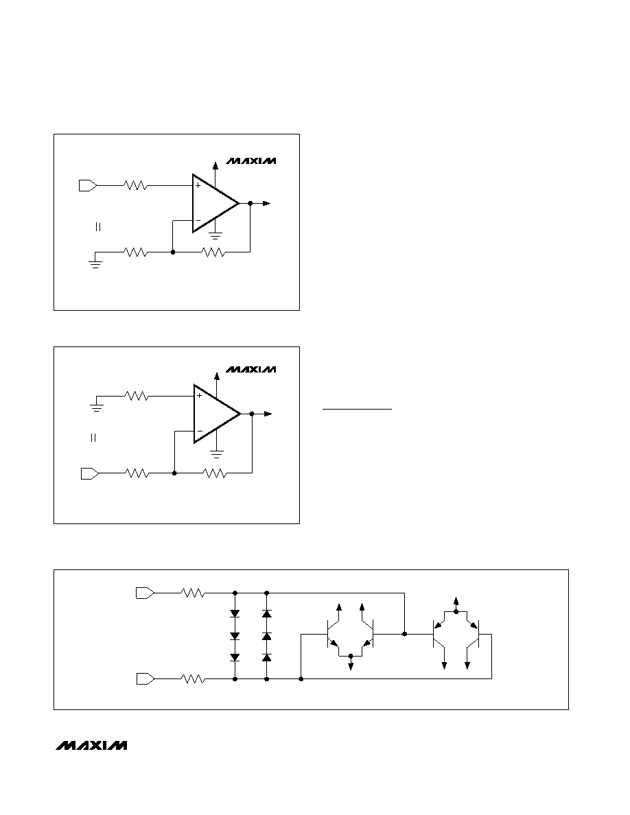
The MAX4040–MAX4044 family’s inputs are protected
from large differential input voltages by internal 2.2k
series resistors and back-to-back triple-diode stacks
across the inputs (Figure 2). For differential input volt-
ages (much less than 1.8V), input resistance is typically
45M
. For differential input voltages greater than 1.8V,
input resistance is around 4.4k
, and the input bias
current can be approximated by the following equation:
IBIAS = (VDIFF - 1.8V) / 4.4k
In the region where the differential input voltage
approaches 1.8V, the input resistance decreases expo-
nentially from 45M
to 4.4k as the diode block begins
conducting. Conversely, the bias current increases with
the same curve.
Rail-to-Rail Output Stage
The MAX4040–MAX4044 output stage can drive up to a
25k
load and still swing to within 60mV of the rails.
Figure 3 shows the output voltage swing of a MAX4040
configured as a unity-gain buffer, powered from a single
+4.0V supply voltage. The output for this setup typically
swings from (VEE + 10mV) to (VCC - 10mV) with a 100k
load.
Applications Information
Power-Supply Considerations
The MAX4040–MAX4044 operate from a single +2.4V to
+5.5V supply (or dual ±1.2V to ±2.75V supplies) and
consume only 10A of supply current per amplifier. A
high power-supply rejection ratio of 85dB allows the
amplifiers to be powered directly off a decaying battery
voltage, simplifying design and extending battery life.
Power-Up Settling Time
The MAX4040–MAX4044 typically require 200s to
power up after VCC is stable. During this start-up time,
the output is indeterminant. The application circuit
should allow for this initial delay.
R3
R3 = R1
R2
R1
R2
MAX4040–
MAX4044
VIN
Figure 1b. Minimizing Offset Error Due to Input Bias Current
(Inverting)
2.2k
2.2k
IN-
IN+
Figure 2. Input Protection Circuit
R3
VIN
R3 = R1
R2
R1
R2
MAX4040–
MAX4044
Figure 1a. Minimizing Offset Error Due to Input Bias Current
(Noninverting)
相关PDF资料 |
PDF描述 |
|---|---|
| LMX324AUD+T | IC OP AMP LV R-R QUAD 14TSSOP |
| 81040-660303-RB | CONN HEADER 40POS STR LONG PCB |
| BP/HHD | FUSEHOLDER BLACK FOR ATC BLADE |
| TSW-127-07-G-T | CONN HEADER 81POS .100" TPL |
| RL2512FK-07R015L | RES .015 OHM 1W 1% 2512 SMD |
相关代理商/技术参数 |
参数描述 |
|---|---|
| MAX4041ESA+ | 功能描述:运算放大器 - 运放 uPower Rail-Rail RoHS:否 制造商:STMicroelectronics 通道数量:4 共模抑制比(最小值):63 dB 输入补偿电压:1 mV 输入偏流(最大值):10 pA 工作电源电压:2.7 V to 5.5 V 安装风格:SMD/SMT 封装 / 箱体:QFN-16 转换速度:0.89 V/us 关闭:No 输出电流:55 mA 最大工作温度:+ 125 C 封装:Reel |
| MAX4041ESA+T | 功能描述:运算放大器 - 运放 uPower Rail-Rail RoHS:否 制造商:STMicroelectronics 通道数量:4 共模抑制比(最小值):63 dB 输入补偿电压:1 mV 输入偏流(最大值):10 pA 工作电源电压:2.7 V to 5.5 V 安装风格:SMD/SMT 封装 / 箱体:QFN-16 转换速度:0.89 V/us 关闭:No 输出电流:55 mA 最大工作温度:+ 125 C 封装:Reel |
| MAX4041ESA-T | 功能描述:运算放大器 - 运放 uPower Rail-Rail RoHS:否 制造商:STMicroelectronics 通道数量:4 共模抑制比(最小值):63 dB 输入补偿电压:1 mV 输入偏流(最大值):10 pA 工作电源电压:2.7 V to 5.5 V 安装风格:SMD/SMT 封装 / 箱体:QFN-16 转换速度:0.89 V/us 关闭:No 输出电流:55 mA 最大工作温度:+ 125 C 封装:Reel |
| MAX4041EUA | 功能描述:运算放大器 - 运放 uPower Rail-Rail RoHS:否 制造商:STMicroelectronics 通道数量:4 共模抑制比(最小值):63 dB 输入补偿电压:1 mV 输入偏流(最大值):10 pA 工作电源电压:2.7 V to 5.5 V 安装风格:SMD/SMT 封装 / 箱体:QFN-16 转换速度:0.89 V/us 关闭:No 输出电流:55 mA 最大工作温度:+ 125 C 封装:Reel |
| MAX4041EUA+ | 功能描述:运算放大器 - 运放 uPower Rail-Rail RoHS:否 制造商:STMicroelectronics 通道数量:4 共模抑制比(最小值):63 dB 输入补偿电压:1 mV 输入偏流(最大值):10 pA 工作电源电压:2.7 V to 5.5 V 安装风格:SMD/SMT 封装 / 箱体:QFN-16 转换速度:0.89 V/us 关闭:No 输出电流:55 mA 最大工作温度:+ 125 C 封装:Reel |
发布紧急采购,3分钟左右您将得到回复。