- 您现在的位置:买卖IC网 > PDF目录2157 > MAX4044ESD+T (Maxim Integrated Products)IC OP AMP R-R QUAD 14-SOIC PDF资料下载
参数资料
| 型号: | MAX4044ESD+T |
| 厂商: | Maxim Integrated Products |
| 文件页数: | 9/16页 |
| 文件大小: | 0K |
| 描述: | IC OP AMP R-R QUAD 14-SOIC |
| 标准包装: | 2,500 |
| 放大器类型: | 通用 |
| 电路数: | 4 |
| 输出类型: | 满摆幅 |
| 转换速率: | 0.04 V/µs |
| 增益带宽积: | 90kHz |
| 电流 - 输入偏压: | 2nA |
| 电压 - 输入偏移: | 200µV |
| 电流 - 电源: | 14µA |
| 电流 - 输出 / 通道: | 2.5mA |
| 电压 - 电源,单路/双路(±): | 2.4 V ~ 5.5 V,±1.2 V ~ 2.75 V |
| 工作温度: | -40°C ~ 85°C |
| 安装类型: | 表面贴装 |
| 封装/外壳: | 14-SOIC(0.154",3.90mm 宽) |
| 供应商设备封装: | 14-SOIC |
| 包装: | 带卷 (TR) |
MAX4040–MAX4044
Single/Dual/Quad, Low-Cost, SOT23,
Micropower, Rail-to-Rail I/O Op Amps
2
_______________________________________________________________________________________
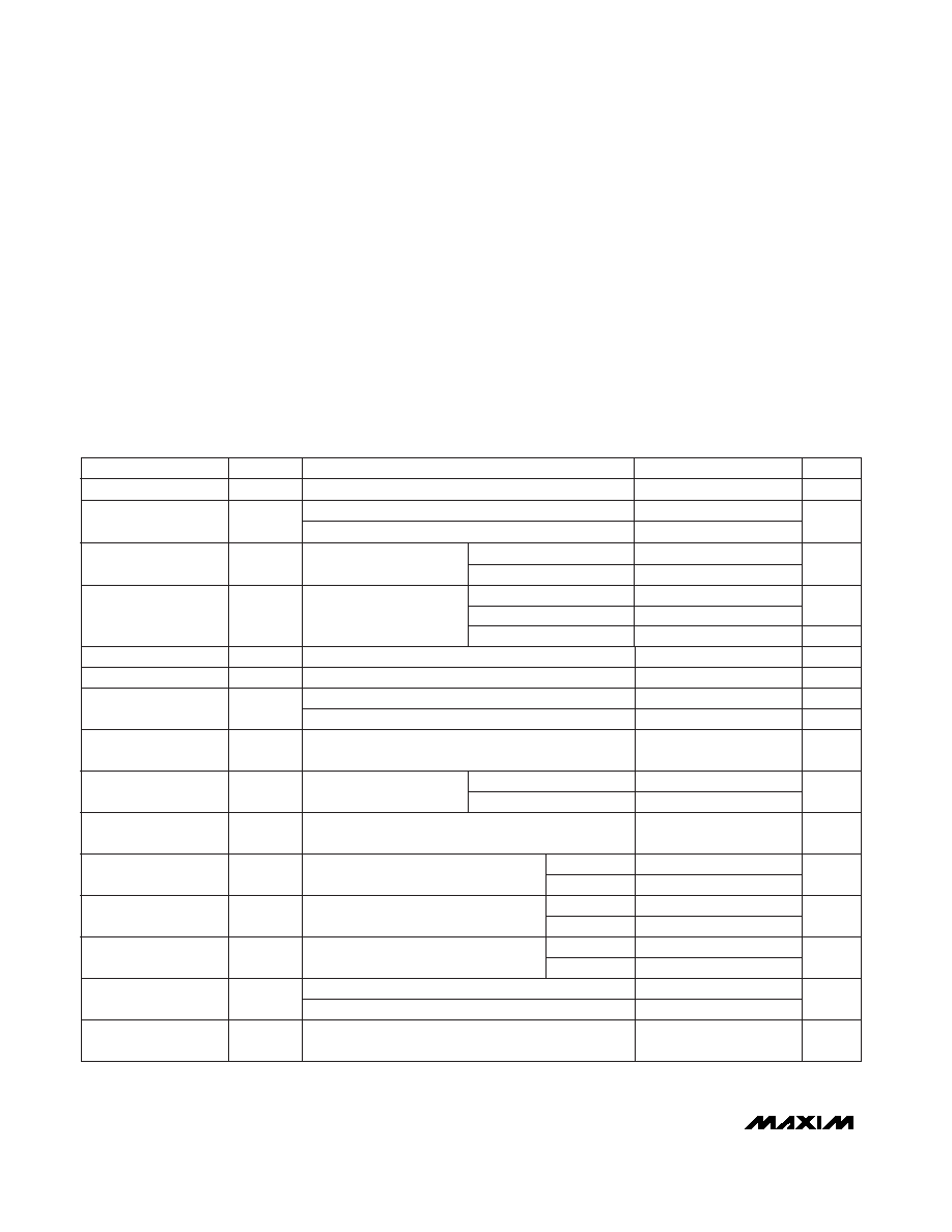
ABSOLUTE MAXIMUM RATINGS
ELECTRICAL CHARACTERISTICS—TA = +25°C
(VCC = +5.0V, VEE = 0V, VCM = 0V, VOUT = VCC / 2, SHDN = VCC, RL = 100k
tied to VCC / 2, unless otherwise noted.)
Stresses beyond those listed under “Absolute Maximum Ratings” may cause permanent damage to the device. These are stress ratings only, and functional
operation of the device at these or any other conditions beyond those indicated in the operational sections of the specifications is not implied. Exposure to
absolute maximum rating conditions for extended periods may affect device reliability.
Supply Voltage (VCC to VEE)..................................................+6V
All Other Pins ...................................(VCC + 0.3V) to (VEE - 0.3V)
Output Short-Circuit Duration to VCC or VEE ..............Continuous
Continuous Power Dissipation (TA = +70°C)
5-Pin SOT23 (derate 7.1mW/°C above +70°C).............571mW
8-Pin MAX (derate 4.1mW/°C above +70°C) ..............330mW
8-Pin SO (derate 5.88mW/°C above +70°C).................471mW
10-Pin MAX (derate 5.6mW/°C above +70°C) ...........444mW
14-Pin SO (derate 8.33mW/°C above +70°C)..............667mW
Operating Temperature Range ...........................-40°C to +85°C
Junction Temperature ......................................................+150°C
Storage Temperature Range .............................-65°C to +160°C
Lead Temperature (soldering, 10s) .................................+300°C
14
20
VCC = 5.0V
(Note 1)
Input Offset Current
IOS
±0.5
±3.0
nA
(Note 1)
VIN+ - VIN- < 1.0V
Differential Input
Resistance
RIN(DIFF)
45
M
2.0
5.0
VIN+ - VIN- > 2.5V
SHDN = VEE, MAX4041
and MAX4043 only
Large-Signal
Voltage Gain
Shutdown Supply
Current per Amplifier
ICC(SHDN)
1.0
Supply-Voltage Range
VCC
2.4
5.5
V
Inferred from PSRR test
Output Voltage
Swing High
4.4
k
VOH
Inferred from the CMRR test
mV
AVOL
dB
PARAMETER
SYMBOL
MIN
TYP
MAX
UNITS
Supply Current
per Amplifier
ICC
10
A
94
VCC = 2.4V
10
Specified as
VCC - VOH
Power-Supply
Rejection Ratio
PSRR
dB
(VEE + 0.2V)
≤ VOUT ≤ (VCC - 0.2V)
60
90
74
85
Output Voltage
Swing Low
Input Common-Mode
Voltage Range
RL = 100k
RL = 25k
RL = 100k
RL = 25k
A
VCM
VEE
VCC
V
2.4V
≤ VCC ≤ 5.5V
75
85
VCC = 2.4V
VOL
mV
10
Specified as
VEE - VOL
Input Bias Current
IB
±2
±10
nA
40
60
RL = 100k
RL = 25k
Output Short-Circuit
Current
IOUT(SC)
mA
0.7
Sourcing
2.5
Channel-to-Channel
Isolation
Sinking
dB
CONDITIONS
80
Specified at DC, MAX4042/MAX4043/MAX4044 only
VCC = 5.0V
±0.20
±2.0
VOS
Input Offset Voltage
mV
±0.25
±2.5
VEE
≤ VCM ≤ VCC
70
94
dB
CMRR
Common-Mode
Rejection Ratio
MAX404_EU_
All other packages
65
94
VEE
≤ VCM ≤ VCC
MAX4044ESD
MAX404_EU_
All other packages
mV
±0.20
±1.50
相关PDF资料 |
PDF描述 |
|---|---|
| MAX4069AUB+T | IC AMP CURRENT SENSE 10-UMAX |
| MAX4073HAUT+T | IC AMP CURRENT SENSE SOT23-6 |
| MAX4075BNEUA+T | IC OPAMP DUAL GAIN R/R 8UMAX |
| MAX4080TAUA/V+T | IC AMP CURRENT SENSE 8UMAX |
| MAX4092ASA+ | IC OP AMP DUAL R-R 8-SOIC |
相关代理商/技术参数 |
参数描述 |
|---|---|
| MAX40-45CA | 制造商:MDE 制造商全称:MDE Semiconductor, Inc. 功能描述:HIGH CURRENT TRANSIENT VOLTAGE SUPPRESSOR (TVS) DIODE STAND-OFF VOLTAGE 12 TO 150 Volts 40000 Watt Peak Pulse Power |
| MAX40-48CA | 制造商:MDE 制造商全称:MDE Semiconductor, Inc. 功能描述:HIGH CURRENT TRANSIENT VOLTAGE SUPPRESSOR (TVS) DIODE STAND-OFF VOLTAGE 12 TO 150 Volts 40000 Watt Peak Pulse Power |
| MAX404C/D | 制造商:MAXIM 制造商全称:Maxim Integrated Products 功能描述:Video Operational Amplifier |
| MAX404CPA | 制造商:Rochester Electronics LLC 功能描述: 制造商:Maxim Integrated Products 功能描述: |
| MAX404CSA | 制造商:Maxim Integrated Products 功能描述: |
发布紧急采购,3分钟左右您将得到回复。