- 您现在的位置:买卖IC网 > PDF目录10352 > MAX4060ETA+T (Maxim Integrated Products)IC PREAMP AUDIO STER AB 8TDFN PDF资料下载
参数资料
| 型号: | MAX4060ETA+T |
| 厂商: | Maxim Integrated Products |
| 文件页数: | 8/15页 |
| 文件大小: | 0K |
| 描述: | IC PREAMP AUDIO STER AB 8TDFN |
| 产品培训模块: | Lead (SnPb) Finish for COTS Obsolescence Mitigation Program |
| 标准包装: | 2,500 |
| 类型: | AB 类 |
| 输出类型: | 2 通道(立体声) |
| 电源电压: | 4.5 V ~ 5.5 V |
| 特点: | 差分输入,麦克风 |
| 安装类型: | 表面贴装 |
| 供应商设备封装: | 8-TDFN-EP(3x3) |
| 封装/外壳: | 8-WDFN 裸露焊盘 |
| 包装: | 带卷 (TR) |
MAX4060/MAX4061/MAX4062
Differential Microphone Preamplifiers with
Internal Bias and Complete Shutdown
2
_______________________________________________________________________________________
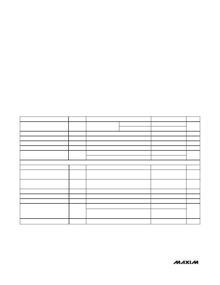
ABSOLUTE MAXIMUM RATINGS
ELECTRICAL CHARACTERISTICS
(VCC = 3V for MAX4061/MAX4062, VCC = 5V for MAX4060, VGND = 0V, VSHDN = VCC, VINT/AUX = 0V, RG = 11.11kΩ,
RL = 100k
Ω to 1.5V, RBIAS = ∞, TA = TMIN to TMAX, unless otherwise noted. Typical values are at TA = +25°C.) (Notes 1, 2)
Stresses beyond those listed under “Absolute Maximum Ratings” may cause permanent damage to the device. These are stress ratings only, and functional
operation of the device at these or any other conditions beyond those indicated in the operational sections of the specifications is not implied. Exposure to
absolute maximum rating conditions for extended periods may affect device reliability.
Supply Voltage (VCC to GND). .................................-0.3V to +6V
Any Other Pin to GND ................................-0.3V to (VCC + 0.3V)
Duration of Short Circuit to GND or VCC ....................Continuous
Continuous Input Current (any pin) ................................ ±10mA
Continuous Power Dissipation (TA = +70°C)
8-Pin TDFN (derate 24.4mW/°C above +70°C) ......1951.2mW
8-Bump MAX (derate 4.8mW/°C above +70°C) .....387.8mW
10-Bump MAX (derate 8.8mW/°C above +70°C) ..707.3mW
Operating Temperature Range ...........................-40°C to +85°C
Junction Temperature ......................................................+150°C
Storage Temperature Range .............................-65°C to +150°C
Lead Temperature (soldering, 10s) .................................+300°C
Soldering Temperature (reflow) .......................................+260°C
PARAMETER
SYMBOL
CONDITIONS
MIN
TYP
MAX
UNITS
MAX4061/MAX4062
2.4
5.5
Supply Voltage Range
VCC
Inferred from
PSRR test
MAX4060
4.5
5.5
V
Supply Current
ICC
0.75
1.2
mA
Output Common-Mode Voltage
VOCM
1.25
1.5
1.75
V
Slew Rate
SR
AV = 10V/V
±1
V/s
Supply Current in Shutdown
ISHDN
VSHDN = 0V, MAX4061
0.001
1
A
To GND
30
Output Short-Circuit Current
ISC
To VCC
30
mA
DIFFERENTIAL INPUT (VINT/AUX = 0V for MAX4060/MAX4062, default for MAX4061)
Input Offset Voltage
VOS
±0.1
±5mV
Common-Mode Input Voltage
Range
VCM
12
V
Maximum Differential Input
Voltage
VDIFFMAX
AV = 1V/V, MAX4061/MAX4062
1
V
Small-Signal Bandwidth
BW-3dB
600
kHz
Input Resistance
RIN
Either differential input
100
k
Ω
Input Resistance Match
RMATCH
1%
AV = 10V/V, f = 1kHz
100
Input Noise-Voltage Density
en
AV = 100V/V, f = 1kHz, MAX4061/MAX4062
only
20
nV/
√Hz
RMS Output Noise Voltage
VNRMS
AV = 10V/V, BW = 22Hz to 22kHz
125
VRMS
相关PDF资料 |
PDF描述 |
|---|---|
| D38999/20FJ61PNLC | CONN HSG RCPT 61POS WALL MT PINS |
| MAX4061ETA+T | IC PREAMP AUDIO MONO AB 8TDFN |
| D38999/20WJ61PNLC | CONN HSG RCPT 61POS WALL MT PINS |
| V150A28C500BL | CONVERTER MOD DC/DC 28V 500W |
| MAX9724BEBC+TG45 | IC AMP AUDIO .045W STER 12UCSP |
相关代理商/技术参数 |
参数描述 |
|---|---|
| MAX4060EUA | 制造商:Maxim Integrated Products 功能描述:DIFFERENTIAL MICROPHONE PREAMPLIFIERS WITH IN - Rail/Tube |
| MAX4060EVKIT | 制造商:MAXIM 制造商全称:Maxim Integrated Products 功能描述:Evaluation Kit for the MAX4060 |
| MAX4060-MAX4062 | 制造商:MAXIM 制造商全称:Maxim Integrated Products 功能描述:Differential Microphone Preamplifiers with Internal Bias and Complete Shutdown |
| MAX4061 | 制造商:MAXIM 制造商全称:Maxim Integrated Products 功能描述:Differential Microphone Preamplifiers with Internal Bias and Complete Shutdown |
| MAX4061EGA | 制造商:Maxim Integrated Products 功能描述:DIFFERENTIAL MICROPHONE PREAMPLIFIERS WITH IN - Rail/Tube |
发布紧急采购,3分钟左右您将得到回复。