- 您现在的位置:买卖IC网 > PDF目录2157 > MAX4117ESA+T (Maxim Integrated Products)IC AMP CURRENT FB LP 8-SOIC PDF资料下载
参数资料
| 型号: | MAX4117ESA+T |
| 厂商: | Maxim Integrated Products |
| 文件页数: | 5/12页 |
| 文件大小: | 0K |
| 描述: | IC AMP CURRENT FB LP 8-SOIC |
| 标准包装: | 2,500 |
| 放大器类型: | 电流反馈 |
| 电路数: | 2 |
| 转换速率: | 1200 V/µs |
| -3db带宽: | 400MHz |
| 电流 - 输入偏压: | 3.5µA |
| 电压 - 输入偏移: | 1000µV |
| 电流 - 电源: | 5mA |
| 电流 - 输出 / 通道: | 80mA |
| 电压 - 电源,单路/双路(±): | ±4.5 V ~ 5.5 V |
| 工作温度: | -40°C ~ 85°C |
| 安装类型: | 表面贴装 |
| 封装/外壳: | 8-SOIC(0.154",3.90mm 宽) |
| 供应商设备封装: | 8-SOIC |
| 包装: | 带卷 (TR) |
MAX4112/MAX4113/MAX4117–MAX4120
Single/Dual/Quad, 400MHz, Low-Power,
Current Feedback Amplifiers
2
_______________________________________________________________________________________
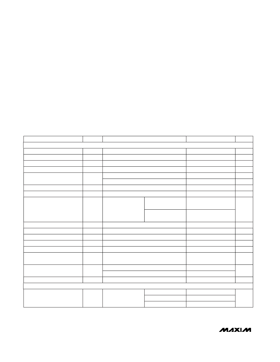
ABSOLUTE MAXIMUM RATINGS
ELECTRICAL CHARACTERISTICS
(VCC = +5V, VEE = -5V, TA = TMIN to TMAX, unless otherwise noted. Typical values are at TA = +25°C.) (Note 1)
Stresses beyond those listed under “Absolute Maximum Ratings” may cause permanent damage to the device. These are stress ratings only, and functional
operation of the device at these or any other conditions beyond those indicated in the operational sections of the specifications is not implied. Exposure to
absolute maximum rating conditions for extended periods may affect device reliability.
Power-Supply Voltage (VCC to VEE).......................................12V
Input Voltage (IN_+, IN_-)...................(VCC + 0.3V) to (VEE - 0.3V)
IN_ _ Current (Note 1) ......................................................±10mA
Short-Circuit Duration (VOUT to GND)
VIN < 1.5V ...............................................................Continuous
VIN > 1.5V ..........................................................................0sec
Continuous Power Dissipation (TA = +70°C)
8-Pin SO (derate 5.88mW/°C above +70°C).................471mW
8-Pin MAX (derate 4.10mW/°C above +70°C) ............330mW
14-Pin SO (derate 8.33mW/°C above +70°C)...............667mW
16-Pin QSOP (derate 9.52mW/°C above +70°C)..........762mW
Operating Temperature Range
MAX41_ _E_ _ ...................................................-40°C to +85°C
Storage Temperature Range .............................-65°C to +160°C
Lead Temperature (soldering, 10s) .................................+300°C
IN+
k
500
VOUT = 0V
MAX4112/MAX4117/
MAX4119
VOUT = 0V
RL = 30, TA = 0°C to +85°C
IN-
VIN = 0V
f = 10kHz
VOUT = ±2.0V, VCM = 0V, RL = 100
VS = ±4.5V to ±5.5V
f = 1MHz to 100MHz
f = 10kHz
VOUT = 0V, VIN = -VOS
VCM = ±2.5V
CONDITIONS
30
9
Input Resistance
in+
Positive Input Current Noise
MAX4113/MAX4118/
MAX4120
mA
65
80
IOUT
Output Current Drive
RL = 100
RL = ∞
mA
5
6.5
ISY
Quiescent Supply Current
per Amplifier
k
ZOL
Open-Loop Transimpedance
250
500
V
dB
45
50
CMR
Common-Mode Rejection
V
-2.5
2.5
VCM
Common-Mode Input Voltage
V/°C
10
TCVOS
Input Offset Voltage Drift
mV
18
VOS
Input Offset Voltage
pA/√Hz
14
in-
Negative Input Current Noise
pA/√Hz
13
VRMS
27
EnRMS
Integrated Voltage Noise
nV/√Hz
2.2
en
Input Voltage Noise
A
3.5
20
IB+
Positive Input Bias Current
A
3.5
20
IB-
Negative Input Bias Current
UNITS
MIN
TYP
MAX
SYMBOL
PARAMETER
60
80
PSR
Power-Supply Rejection
±3.1
±3.5
VOUT
Output-Voltage Swing
±3.5
±3.8
VOUT ≤ 0.1VRMS
MHz
400
BWSS
Small-Signal -3dB Bandwidth
300
270
MAX4112/MAX4117
MAX4113/MAX4119
MAX4118/MAX4120
DC SPECIFICATIONS (RL = ∞, unless otherwise noted)
AC SPECIFICATIONS (RL = 100, unless otherwise noted)
相关PDF资料 |
PDF描述 |
|---|---|
| MAX4129ESD+T | IC OP AMP QUAD R-R 14-SOIC |
| MAX4134ESD+T | IC OP AMP QUAD 14-SOIC |
| MAX4147ESD+T | IC RX DIFF LINE HS 14-SOIC |
| MAX414ESD+T | IC OPAMP LN LV PREC 28MHZ 14SOIC |
| MAX4164ESD+T | IC OP AMP R-R I/O SS 14-SOIC |
相关代理商/技术参数 |
参数描述 |
|---|---|
| MAX4117ESA-TG068 | 制造商:Rochester Electronics LLC 功能描述: 制造商:Maxim Integrated Products 功能描述: |
| MAX4117EVKIT | 功能描述:放大器 IC 开发工具 RoHS:否 制造商:International Rectifier 产品:Demonstration Boards 类型:Power Amplifiers 工具用于评估:IR4302 工作电源电压:13 V to 23 V |
| MAX4117EVKIT-SO | 功能描述:放大器 IC 开发工具 RoHS:否 制造商:International Rectifier 产品:Demonstration Boards 类型:Power Amplifiers 工具用于评估:IR4302 工作电源电压:13 V to 23 V |
| MAX4118 | 制造商:MAXIM 制造商全称:Maxim Integrated Products 功能描述:Single/Dual/Quad, 400MHz, Low-Power, Current Feedback Amplifiers |
| MAX4118ESA | 功能描述:高速运算放大器 RoHS:否 制造商:Texas Instruments 通道数量:1 电压增益 dB:116 dB 输入补偿电压:0.5 mV 转换速度:55 V/us 工作电源电压:36 V 电源电流:7.5 mA 最大工作温度:+ 85 C 安装风格:SMD/SMT 封装 / 箱体:SOIC-8 封装:Tube |
发布紧急采购,3分钟左右您将得到回复。