- 您现在的位置:买卖IC网 > PDF目录2157 > MAX4164ESD+T (Maxim Integrated Products)IC OP AMP R-R I/O SS 14-SOIC PDF资料下载
参数资料
| 型号: | MAX4164ESD+T |
| 厂商: | Maxim Integrated Products |
| 文件页数: | 6/13页 |
| 文件大小: | 0K |
| 描述: | IC OP AMP R-R I/O SS 14-SOIC |
| 标准包装: | 2,500 |
| 放大器类型: | 通用 |
| 电路数: | 4 |
| 输出类型: | 满摆幅 |
| 转换速率: | 0.115 V/µs |
| 增益带宽积: | 200kHz |
| 电流 - 输入偏压: | 1pA |
| 电压 - 输入偏移: | 500µV |
| 电流 - 电源: | 25µA |
| 电流 - 输出 / 通道: | 15mA |
| 电压 - 电源,单路/双路(±): | 2.7 V ~ 10 V,±1.35 V ~ 5 V |
| 工作温度: | -40°C ~ 85°C |
| 安装类型: | 表面贴装 |
| 封装/外壳: | 14-SOIC(0.154",3.90mm 宽) |
| 供应商设备封装: | 14-SOIC |
| 包装: | 带卷 (TR) |
MAX4162/MAX4163/MAX4164
UCSP, Micropower, Single-Supply, 10V,
Rail-to-Rail I/O Op Amps
2
_______________________________________________________________________________________
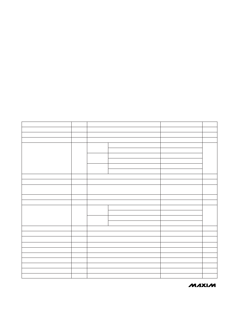
ABSOLUTE MAXIMUM RATINGS
ELECTRICAL CHARACTERISTICS: 3V Operation
(VDD = 3V, VSS = 0V, VCM = VDD/2, VOUT = VDD/2, RL connected to VDD/2, TA = -40°C to +85°C, unless otherwise noted. Typical val-
ues are at TA = +25°C.) (Note 1)
Stresses beyond those listed under “Absolute Maximum Ratings” may cause permanent damage to the device. These are stress ratings only, and functional
operation of the device at these or any other conditions beyond those indicated in the operational sections of the specifications is not implied. Exposure to
absolute maximum rating conditions for extended periods may affect device reliability.
Supply Voltage (VDD to VSS) ..................................................11V
IN+, IN-, OUT Voltage ......................(VDD + 0.3V) to (VSS - 0.3V)
Short-Circuit Duration (to either rail)...........................Continuous
Continuous Power Dissipation (TA = +70°C)
5-Pin SOT23 (derate 3.9mW/°C above +70°C)..............312mW
8-Pin SO (derate 7.4mW/°C above +70°C)....................588mW
8-Pin UCSP (derate 4.7mW/°C above +70°C) ...............379mW
8-Pin MAX (derate 4.8mW/°C above +70°C) ...............387mW
14-Pin SO (derate 12.3mW/°C above +70°C)................987mW
Operating Temperature Range ...........................-40°C to +85°C
Storage Temperature Range .............................-65°C to +150°C
Junction Temperature ......................................................+150°C
Lead Temperature (soldering, 10s) .................................+300°C
Soldering Temperature (reflow, UCSP)............................+260°C
To either supply rail
VOL - VSS
VDD - VOH
VOL - VSS
VDD - VOH
Inferred from PSRR test
RL = 10k
Inferred from CMRR test
TA = +25°C
TA = -40°C to +85°C
TA = +25°C
TA = -40°C to +85°C
CONDITIONS
15
ISC
mV
325
RL = 100k
VOUT
325
30
180
RL = 10k
30
180
dB
AV
85
120
dB
CMRR
70
100
pA
1.0
100
V
2.5
10.0
VDD
IB
T
VSS -
VDD +
0.25
VCM
>10
RIN
±6
±0.5
±5
MAX4164
±0.5
±3
VOS
±4
MAX4162
±0.5
±4
mV
±5
MAX4163
UNITS
MIN
TYP
MAX
SYMBOL
AV = 1V/V
kHz
200
GBWP
VDD = 2.5V to 10V
PSRR
dB
80
110
mA
0.1
ROUT
V
VCM = (VSS - 0.25V) to (VDD + 0.25V)
V/°C
TCVOS
2
TA = +25°C
TA = -40°C to +85°C
A
25
40
IDD
degrees
60
φM
dB
12
GM
VOUT = 1V to 2V step
s
50
VDD = 0 to 3V step, VIN = VDD/2, AV = 1V/V
s
20
tON
V/ms
115
SR
f = 1kHz, VOUT = 2VP-P, RL = 100k, AV = 1V/V
THD
%
0.02
Phase Margin
Gain Margin
Output Short-Circuit Current
Output Voltage Swing
Input Offset Voltage Tempco
Settling Time to 0.1%
Large-Signal Voltage Gain
Supply Current (Per Amplifier)
Turn-On Time
Slew Rate
Total Harmonic Distortion
Common-Mode Rejection Ratio
Operating Voltage Range
Input Bias Current (Note 2)
Input Common-Mode Voltage
Range
Differential Input Resistance
Input Offset Voltage
PARAMETER
Gain-Bandwidth Product
Power-Supply Rejection Ratio
Closed-Loop Output Resistance
相关PDF资料 |
PDF描述 |
|---|---|
| MAX4169ESD+T | IC OP AMP R-R I/O W/SD 14-SOIC |
| MAX4172ESA+T | IC AMP CURRENT SENSE 8-SOIC |
| MAX4173TEUT-T | IC AMP HISIDE CURR V-OUT SOT23-6 |
| MAX4174AOEUK+T | IC OPAMP SGL/DUAL FIXED SOT23-5 |
| MAX4181EUT+T | IC AMP CURRENT SENSE SOT23-6 |
相关代理商/技术参数 |
参数描述 |
|---|---|
| MAX4165 | 制造商:MAXIM 制造商全称:Maxim Integrated Products 功能描述:High-Output-Drive, Precision, Low-Power, Single- Supply, Rail-to-Rail I/O Op Amps with Shutdown |
| MAX4165EUK | 制造商:Maxim Integrated Products 功能描述:OP AMP HIGH O/P RRI/O SMD 4165 |
| MAX4165EUK+ | 制造商:Maxim Integrated Products 功能描述:OP AMP SGL GP R-R I/O 3.25V/6.5V 5PIN SOT-23 - Bulk 制造商:Maxim Integrated Products 功能描述:Bulk 制造商:Maxim Integrated Products 功能描述:OP AMP HIGH O/P RRI/O SMD 4165 |
| MAX4165EUK+T | 功能描述:运算放大器 - 运放 High-Output-Drive Supply Rail-Rail RoHS:否 制造商:STMicroelectronics 通道数量:4 共模抑制比(最小值):63 dB 输入补偿电压:1 mV 输入偏流(最大值):10 pA 工作电源电压:2.7 V to 5.5 V 安装风格:SMD/SMT 封装 / 箱体:QFN-16 转换速度:0.89 V/us 关闭:No 输出电流:55 mA 最大工作温度:+ 125 C 封装:Reel |
| MAX4165EUKT | 制造商:Maxim Integrated Products 功能描述: |
发布紧急采购,3分钟左右您将得到回复。