- 您现在的位置:买卖IC网 > PDF目录3276 > MAX4183ESD+T (Maxim Integrated Products)IC AMP CURRENT SENSE 14-SOIC PDF资料下载
参数资料
| 型号: | MAX4183ESD+T |
| 厂商: | Maxim Integrated Products |
| 文件页数: | 12/24页 |
| 文件大小: | 0K |
| 描述: | IC AMP CURRENT SENSE 14-SOIC |
| 标准包装: | 2,500 |
| 放大器类型: | 电流反馈 |
| 电路数: | 2 |
| 转换速率: | 450 V/µs |
| -3db带宽: | 270MHz |
| 电流 - 输入偏压: | 1µA |
| 电压 - 输入偏移: | 1500µV |
| 电流 - 电源: | 1mA |
| 电流 - 输出 / 通道: | 60mA |
| 电压 - 电源,单路/双路(±): | 4.5 V ~ 11 V,±2.25 V ~ 5.5 V |
| 工作温度: | -40°C ~ 85°C |
| 安装类型: | 表面贴装 |
| 封装/外壳: | 14-SOIC(0.154",3.90mm 宽) |
| 供应商设备封装: | 14-SOIC |
| 包装: | 带卷 (TR) |
MAX4180–MAX4187
Single/Dual/Quad, 270MHz, 1mA, SOT23,
Current-Feedback Amplifiers with Shutdown
2
_______________________________________________________________________________________
1
OUT
SING
TOP VIEW
ABSOLUTE MAXIMUM RATINGS
DC ELECTRICAL CHARACTERISTICS—Dual Supplies
(VCC = +5V, VEE = -5V, VIN+ = 0, SHDN
≥ 3V; TA = TMIN to TMAX, unless otherwise noted. Typical values are at TA = +25°C.) (Note 1)
Stresses beyond those listed under “Absolute Maximum Ratings” may cause permanent damage to the device. These are stress ratings only, and functional
operation of the device at these or any other conditions beyond those indicated in the operational sections of the specifications is not implied. Exposure to
absolute maximum rating conditions for extended periods may affect device reliability.
Supply Voltage (VCC to VEE) .................................................12V
Analog Input Voltage .......................(VEE - 0.3V) to (VCC + 0.3V)
Differential Input Voltage .......................................................±2V
SHDN Input Voltage ........................(VEE - 0.3V) to (VCC + 0.3V)
Short-Circuit Duration (OUT to GND, VCC or VEE).....Continuous
Continuous Power Dissipation (TA = +70°C)
6-Pin SOT23 (derate 7.10mW/°C above +70°C)...........571mW
8-Pin SO (derate 5.88mW/°C above +70°C).................471mW
10-Pin MAX (derate 5.60mW/°C above +70°C) ..........444mW
14-Pin SO (derate 8.33mW/°C above +70°C)...............667mW
16-Pin QSOP (derate 8.30mW/°C above +70°C)..........667mW
Operating Temperature Range ...........................-40°C to +85°C
Storage Temperature Range .............................-65°C to +150°C
Lead Temperature (soldering, 10s) .................................+300°C
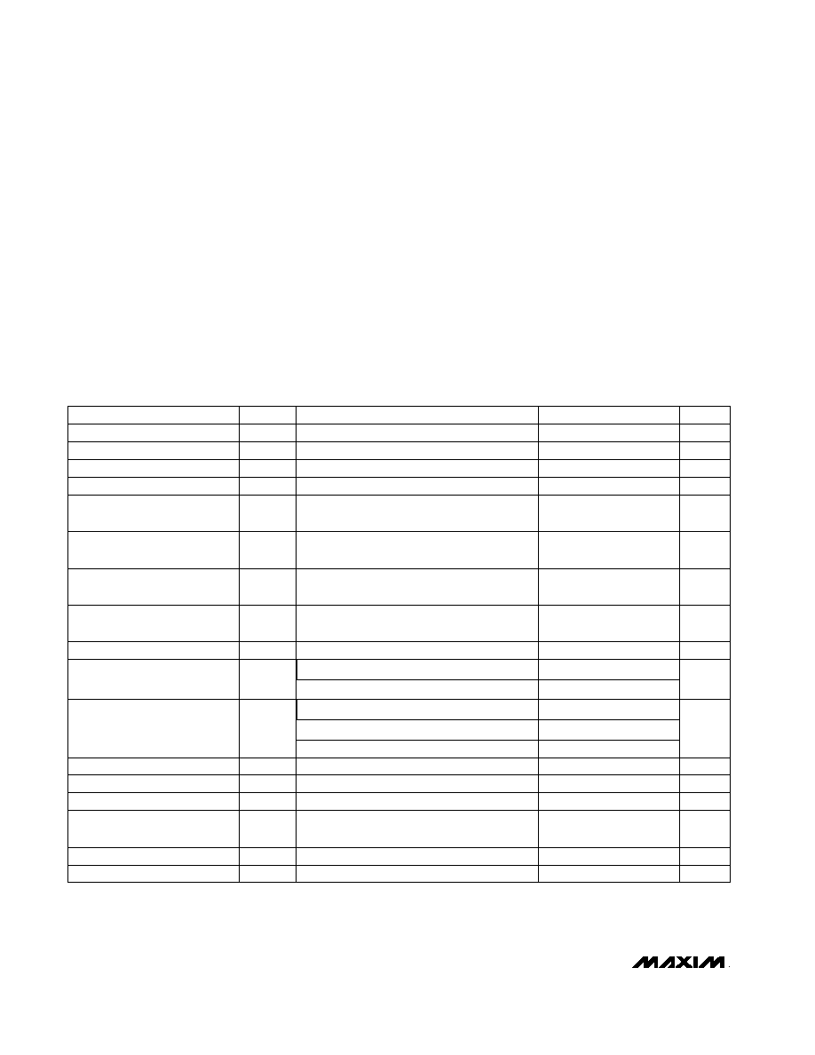
SHDN Logic High Threshold
VIH
VCC - 2.0
V
(Notes 3, 4)
Open-Loop Transresistance
Input Bias Current
(Negative Input)
IB-
±1
±12
A
250
800
PARAMETER
SYMBOL
MIN
TYP
MAX
UNITS
Input Bias Current
(Positive Input)
IB+
Input Offset-Voltage Matching
±1
±7
k
Input Resistance
(Positive Input)
RIN+
Input Resistance
(Negative Input)
RIN-
160
Input Offset Voltage
Input Voltage Range
VCM
±3.6
±3.9
V
VOS
±1.5
±7
mV
Input Offset-Voltage Drift
TCVOS
±12
V/°C
Common-Mode Rejection Ratio
CMRR
-50
-58
dB
TR
0.8
3.0
M
0.3
0.9
Output Voltage Swing
VSW
±3.75
±4.0
V
±3.0
±3.3
±3.0
Output Short-Circuit Current
ISC
±80
mA
Output Resistance
ROUT
0.2
Disabled Output Leakage
Current
IOUT(OFF)
±0.1
±6.0
A
SHDN Logic Low Threshold
VIL
VCC - 3.0
V
CONDITIONS
-3.6V
≤ VCM ≤ 3.6V
MAX4182–MAX4187
RL = 1k
, VOUT = ±3.6V
RL = 150
, VOUT = ±2.5V
-3.6V
≤ VIN+ ≤ 3.6V, -1V ≤ (VIN+ - VIN-) ≤ 1V
RL = 1k
RL = 150
RL = 100
Guaranteed by CMRR test
VCM = 0
SHDN
≤ VIL, VOUT ≤ ±3V (Notes 2, 4)
(Notes 3, 4)
mV
Output Current
IOUT
±32
±60
mA
RL = 30
相关PDF资料 |
PDF描述 |
|---|---|
| MAX4175AGEUK+T | IC OP AMP FIX GAIN SOT23-5 |
| MAX4174AKEUK+T | IC OP AMP FIX GAIN SOT23-5 |
| MAX4180EUT+T | IC AMP CURRENT SENSE SOT23-6 |
| MAX4182ESA+T | IC AMP CURRENT SENSE 8-SOIC |
| MAX4181ESA+T | IC AMP CURRENT SENSE 8-SOIC |
相关代理商/技术参数 |
参数描述 |
|---|---|
| MAX4183EUB | 功能描述:视频放大器 RoHS:否 制造商:ON Semiconductor 通道数量:4 电源类型: 工作电源电压:3.3 V, 5 V 电源电流: 最小工作温度: 最大工作温度: 封装 / 箱体:TSSOP-14 封装:Reel |
| MAX4183EUB+ | 功能描述:视频放大器 RoHS:否 制造商:ON Semiconductor 通道数量:4 电源类型: 工作电源电压:3.3 V, 5 V 电源电流: 最小工作温度: 最大工作温度: 封装 / 箱体:TSSOP-14 封装:Reel |
| MAX4183EUB+T | 功能描述:视频放大器 RoHS:否 制造商:ON Semiconductor 通道数量:4 电源类型: 工作电源电压:3.3 V, 5 V 电源电流: 最小工作温度: 最大工作温度: 封装 / 箱体:TSSOP-14 封装:Reel |
| MAX4183EUB-T | 功能描述:视频放大器 RoHS:否 制造商:ON Semiconductor 通道数量:4 电源类型: 工作电源电压:3.3 V, 5 V 电源电流: 最小工作温度: 最大工作温度: 封装 / 箱体:TSSOP-14 封装:Reel |
| MAX4184 | 制造商:MAXIM 制造商全称:Maxim Integrated Products 功能描述:Evaluation Kit for the MAX687/MAX688/MAX689[MAX687EVKIT/MAX688EVKIT/MAX689EVKIT ] |
发布紧急采购,3分钟左右您将得到回复。