- 您现在的位置:买卖IC网 > PDF目录16898 > MAX4206EVKIT+ (Maxim Integrated Products)EVAL KIT MAX4206 PDF资料下载
参数资料
| 型号: | MAX4206EVKIT+ |
| 厂商: | Maxim Integrated Products |
| 文件页数: | 10/17页 |
| 文件大小: | 0K |
| 描述: | EVAL KIT MAX4206 |
| 标准包装: | 1 |
| 系列: | * |
MAX4206
Precision Transimpedance Logarithmic
Amplifier with Over 5 Decades of Dynamic Range
2
_______________________________________________________________________________________
ABSOLUTE MAXIMUM RATINGS
Stresses beyond those listed under “Absolute Maximum Ratings” may cause permanent damage to the device. These are stress ratings only, and functional
operation of the device at these or any other conditions beyond those indicated in the operational sections of the specifications is not implied. Exposure to
absolute maximum rating conditions for extended periods may affect device reliability.
(All voltages referenced to GND, unless otherwise noted.)
VCC .........................................................................-0.3V to +12V
VEE............................................................................-6V to +0.3V
Supply Voltage (VCC to VEE) .............................................. +12V
REFVOUT ....................................................(VEE - 0.3V) to +3.0V
OSADJ, SCALE, REFISET ...........................(VEE - 0.3V) to +5.5V
REFIIN, LOGIIN ........................................(VEE - 0.3V) to VCMVIN
LOGV1, LOGV2, CMVOUT,
REFIOUT ......................................(VEE - 0.3V) to (VCC + 0.3V)
CMVIN............................................................(VEE - 0.3V) to +1V
Continuous Current (REFIIN, LOGIIN) ................................10mA
Continuous Power Dissipation (TA = +70°C)
16-Pin Thin QFN (derate 16.9mW/°C above +70°C) ....1349mW
Operating Temperature Range ...........................-40°C to +85°C
Junction Temperature .....................................................+150°C
Storage Temperature Range .............................-65°C to +150°C
Lead Temperature (soldering, 10s) .................................+300°C
DC ELECTRICAL CHARACTERISTICS—Single-Supply Operation
(VCC = +5V, VEE = GND = 0V, IREF = 1A, ILOG = 10A, LOGV2 = SCALE, LOGV1 = OSADJ, CMVIN = CMVOUT, RSET > 1M,
TA = -40°C to +85°C. Typical values are at TA = +25°C, unless otherwise noted.) (Note 1)
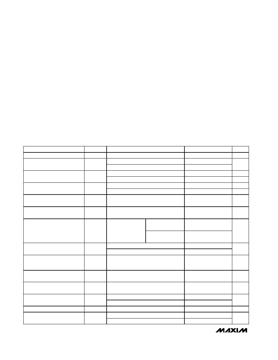
PARAMETER
SYMBOL
CONDITIONS
MIN
TYP
MAX
UNITS
Supply Voltage
VCC
(Note 2)
2.7
11.0
V
TA = +25°C
3.9
5
Supply Current
ICC
TA = -40°C to +85°C
7
mA
Minimum
10
nA
LOGIIN Current Range (Notes 3, 4)
ILOG
Maximum
1
mA
Minimum
10
nA
REFIIN Current Range (Notes 3, 4)
IREF
Maximum
1
mA
Common-Mode Voltage
VCMVOUT
480
500
520
mV
Common-Mode Voltage Input
Range
VCMVIN
0.5
1.0
V
TA = +25°C
±2
±5
Log Conformity Error
VLC
IREF = 10nA,
ILOG= 10nA to 1mA,
K = 0.25V/decade
(Note 4)
TA = -40°C to +85°C
±10
mV
TA = +25°C
237.5
250
262.5
Logarithmic Slope (Scale Factor)
K
TA = -40°C to +85°C (Note 4)
231.25
268.75
mV/
decade
Logarithmic Slope (Scale Factor)
Temperature Drift
TA = -40°C to +85°C
80
V/
decade/
°C
Input Offset Voltage
VIO
TA = +25°C, |VCMVIN - VREFIIN|,
|VCMVIN - VLOGIIN|
15
mV
Input Offset Voltage Temperature
Drift
VIOS
|VCMVIN - VREFIIN|, |VCMVIN - VLOGIIN|6
V/°C
TA = +25°C
1.218
1.238
1.258
Voltage Reference Output
VREFVOUT
TA = -40°C to +85°C (Note 4)
1.195
1.275
V
Voltage Reference Output Current
IREFVOUT
1mA
TA = +25°C
490
500
510
Current Reference Output VoltageVREFISET
TA = -40°C to +85°C (Note 4)
482
518
mV
相关PDF资料 |
PDF描述 |
|---|---|
| SDS130R-472N | INDUCTOR PWR SHIELDED 4.7UH SMD |
| LM4040AEX3-3.3+T | IC VREF SHUNT PREC 3.3V SC-70-3 |
| MAX4073EVKIT+ | EVALUATION KIT FOR MAX4073 |
| 202D163-4-60/42-0 | BOOT MOLDED |
| 202D163-3-60/42-0 | BOOT MOLDED |
相关代理商/技术参数 |
参数描述 |
|---|---|
| MAX4206EVKIT+ | 功能描述:放大器 IC 开发工具 MAX4206 EVAL KIT RoHS:否 制造商:International Rectifier 产品:Demonstration Boards 类型:Power Amplifiers 工具用于评估:IR4302 工作电源电压:13 V to 23 V |
| MAX4207ETE | 功能描述:对数放大器 Transimpedance w/ 100Db Dynamic Range RoHS:否 制造商:Texas Instruments 通道数量:3 带宽:3 dB 共模抑制比(最小值): 输入补偿电压:+/- 7 mV 输入电压范围(最大值):5.5 V 工作电源电压:4.5 V to 5.5 V 电源电流:+/- 15 mA 工作温度范围:- 40 C to +85 C 安装风格:SMD/SMT 封装 / 箱体:VQFN-16 封装:Reel |
| MAX4207ETE+ | 功能描述:对数放大器 Transimpedance w/ 100Db Dynamic Range RoHS:否 制造商:Texas Instruments 通道数量:3 带宽:3 dB 共模抑制比(最小值): 输入补偿电压:+/- 7 mV 输入电压范围(最大值):5.5 V 工作电源电压:4.5 V to 5.5 V 电源电流:+/- 15 mA 工作温度范围:- 40 C to +85 C 安装风格:SMD/SMT 封装 / 箱体:VQFN-16 封装:Reel |
| MAX4207ETE+T | 功能描述:对数放大器 Transimpedance w/ 100Db Dynamic Range RoHS:否 制造商:Texas Instruments 通道数量:3 带宽:3 dB 共模抑制比(最小值): 输入补偿电压:+/- 7 mV 输入电压范围(最大值):5.5 V 工作电源电压:4.5 V to 5.5 V 电源电流:+/- 15 mA 工作温度范围:- 40 C to +85 C 安装风格:SMD/SMT 封装 / 箱体:VQFN-16 封装:Reel |
| MAX4207ETE-T | 功能描述:对数放大器 Transimpedance w/ 100Db Dynamic Range RoHS:否 制造商:Texas Instruments 通道数量:3 带宽:3 dB 共模抑制比(最小值): 输入补偿电压:+/- 7 mV 输入电压范围(最大值):5.5 V 工作电源电压:4.5 V to 5.5 V 电源电流:+/- 15 mA 工作温度范围:- 40 C to +85 C 安装风格:SMD/SMT 封装 / 箱体:VQFN-16 封装:Reel |
发布紧急采购,3分钟左右您将得到回复。