参数资料
| 型号: | MAX4243EUB+ |
| 厂商: | Maxim Integrated Products |
| 文件页数: | 5/16页 |
| 文件大小: | 0K |
| 描述: | IC OP AMP BTR 10-UMAX |
| 产品培训模块: | Lead (SnPb) Finish for COTS Obsolescence Mitigation Program |
| 标准包装: | 50 |
| 系列: | Beyond-the-Rails™ |
| 放大器类型: | 通用 |
| 电路数: | 2 |
| 输出类型: | 满摆幅 |
| 转换速率: | 0.04 V/µs |
| 增益带宽积: | 90kHz |
| 电流 - 输入偏压: | 2nA |
| 电压 - 输入偏移: | 250µV |
| 电流 - 电源: | 14µA |
| 电流 - 输出 / 通道: | 2.5mA |
| 电压 - 电源,单路/双路(±): | 1.8 V ~ 5.5 V,±0.9 V ~ 2.5 V |
| 工作温度: | -40°C ~ 85°C |
| 安装类型: | 表面贴装 |
| 封装/外壳: | 10-TFSOP,10-MSOP(0.118",3.00mm 宽) |
| 供应商设备封装: | 10-µMAX |
| 包装: | 管件 |
| 产品目录页面: | 1388 (CN2011-ZH PDF) |
Single/Dual/Quad, +1.8V/10A, SOT23,
Beyond-the-Rails Op Amps
value, based on driving the output voltage to within
and VEE supplies should be bypassed to ground with
50mV, 100mV, and 200mV of either power-supply rail.
separate 100nF capacitors.
For example, a MAX4241 running from a single +1.8V
Good PC board layout techniques optimize perfor-
supply, operating at TA = +25°C, can source 240A to
mance by decreasing the amount of stray capacitance
within 100mV of VCC and is capable of driving a 7kΩ
at the op amp’s inputs and output. To decrease stray
load resistor to VEE:
capacitance, minimize trace lengths by placing exter-
nal components as close as possible to the op amp.
1.8V - 0.1V
Surface-mount components are an excellent choice.
RL =
= 7kΩ to VEE
240 A
The same application can drive a 3.3k
Ω load resistor
when terminated in VCC / 2 (+0.9V in this case).
Driving Capacitive Loads
The MAX4240–MAX4244 are unity-gain stable for loads
up to 200pF (see Load Resistor vs. Capacitive Load
graph in
Typical Operating Characteristics). Applica-
tions that require greater capacitive drive capability
should use an isolation resistor between the output and
the capacitive load (Figure 8). Note that this alternative
results in a loss of gain accuracy because RISO forms a
voltage divider with the load resistor.
Power-Supply Bypassing and Layout
The MAX4240–MAX4244 family operates from either a
single +1.8V to +5.5V supply or dual ±0.9V to ±2.75V
supplies. For single-supply operation, bypass the
power supply with a 100nF capacitor to VEE (in this
case GND). For dual-supply operation, both the VCC
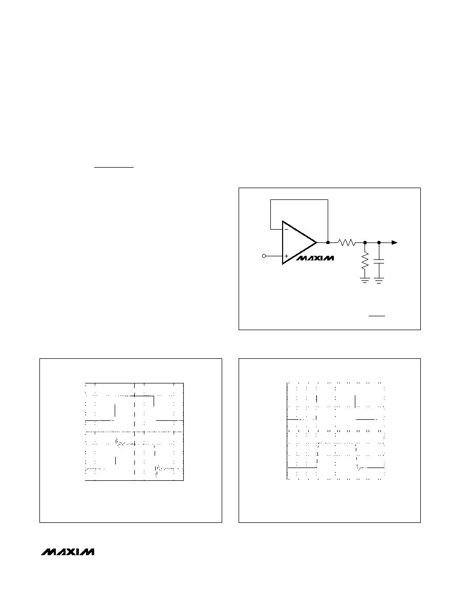
Figure 8a Using a Resistor to Isolate a Capacitive Load from
the Op Amp
RISO
CL
RL
MAX4240
MAX4241
MAX4242
MAX4243
MAX4244
AV =
RL
≈ 1
RL + RISO
50mV/div
IN
OUT
50mV/div
MAX4240-44 fig08b
100
s/div
RISO = NONE, RL = 100kΩ, CL = 700pF
50mV/div
IN
OUT
50mV/div
MAX4240-44 fig08c
100
s/div
RISO = 1kΩ, RL = 100kΩ, CL = 700pF
MAX4240–MAX424
4
Figure 8b. Pulse Response without Isolating Resistor
Figure 8c. Pulse Response with Isolating Resistor
______________________________________________________________________________________
13
相关PDF资料 |
PDF描述 |
|---|---|
| PCF0805R-348KBT1 | RES 348K OHM 0.1W 0805 0.1% SMD |
| MAX4203ESA+ | IC BUFFER OPEN LOOP 8-SOIC |
| 170M4313 | FUSE 450A 690V 1E/86 AR UC |
| MAX4354EUD+ | IC OP AMP R-R SS 14-TSSOP |
| 170M4312 | FUSE 400A 690V 1E/86 AR UC |
相关代理商/技术参数 |
参数描述 |
|---|---|
| MAX4243EUB+ | 功能描述:运算放大器 - 运放 1.8V 10uA Beyond the-Rails RoHS:否 制造商:STMicroelectronics 通道数量:4 共模抑制比(最小值):63 dB 输入补偿电压:1 mV 输入偏流(最大值):10 pA 工作电源电压:2.7 V to 5.5 V 安装风格:SMD/SMT 封装 / 箱体:QFN-16 转换速度:0.89 V/us 关闭:No 输出电流:55 mA 最大工作温度:+ 125 C 封装:Reel |
| MAX4243EUB+T | 功能描述:运算放大器 - 运放 1.8V 10uA Beyond the-Rails RoHS:否 制造商:STMicroelectronics 通道数量:4 共模抑制比(最小值):63 dB 输入补偿电压:1 mV 输入偏流(最大值):10 pA 工作电源电压:2.7 V to 5.5 V 安装风格:SMD/SMT 封装 / 箱体:QFN-16 转换速度:0.89 V/us 关闭:No 输出电流:55 mA 最大工作温度:+ 125 C 封装:Reel |
| MAX4243EUB-T | 功能描述:运算放大器 - 运放 1.8V 10uA Beyond the-Rails RoHS:否 制造商:STMicroelectronics 通道数量:4 共模抑制比(最小值):63 dB 输入补偿电压:1 mV 输入偏流(最大值):10 pA 工作电源电压:2.7 V to 5.5 V 安装风格:SMD/SMT 封装 / 箱体:QFN-16 转换速度:0.89 V/us 关闭:No 输出电流:55 mA 最大工作温度:+ 125 C 封装:Reel |
| MAX4244ESD | 功能描述:运算放大器 - 运放 1.8V 10uA Beyond the-Rails RoHS:否 制造商:STMicroelectronics 通道数量:4 共模抑制比(最小值):63 dB 输入补偿电压:1 mV 输入偏流(最大值):10 pA 工作电源电压:2.7 V to 5.5 V 安装风格:SMD/SMT 封装 / 箱体:QFN-16 转换速度:0.89 V/us 关闭:No 输出电流:55 mA 最大工作温度:+ 125 C 封装:Reel |
| MAX4244ESD+ | 功能描述:运算放大器 - 运放 1.8V 10uA Beyond the-Rails RoHS:否 制造商:STMicroelectronics 通道数量:4 共模抑制比(最小值):63 dB 输入补偿电压:1 mV 输入偏流(最大值):10 pA 工作电源电压:2.7 V to 5.5 V 安装风格:SMD/SMT 封装 / 箱体:QFN-16 转换速度:0.89 V/us 关闭:No 输出电流:55 mA 最大工作温度:+ 125 C 封装:Reel |
发布紧急采购,3分钟左右您将得到回复。