- 您现在的位置:买卖IC网 > PDF目录5520 > MAX4270ESD (Maxim Integrated Products)IC OPAMP DUAL 350MHZ 14-SOIC PDF资料下载
参数资料
| 型号: | MAX4270ESD |
| 厂商: | Maxim Integrated Products |
| 文件页数: | 5/19页 |
| 文件大小: | 0K |
| 描述: | IC OPAMP DUAL 350MHZ 14-SOIC |
| 产品培训模块: | Lead (SnPb) Finish for COTS Obsolescence Mitigation Program |
| 标准包装: | 50 |
| 放大器类型: | 电压反馈 |
| 电路数: | 2 |
| 转换速率: | 900 V/µs |
| 增益带宽积: | 1GHz |
| -3db带宽: | 200MHz |
| 电流 - 输入偏压: | 3.5µA |
| 电压 - 输入偏移: | 1000µV |
| 电流 - 电源: | 28mA |
| 电流 - 输出 / 通道: | 45mA |
| 电压 - 电源,单路/双路(±): | 4.5 V ~ 8 V,±2.25 V ~ 4 V |
| 工作温度: | -40°C ~ 85°C |
| 安装类型: | 表面贴装 |
| 封装/外壳: | 14-SOIC(0.154",3.90mm 宽) |
| 供应商设备封装: | 14-SOIC |
| 包装: | 管件 |
MAX4265–MAX4270
Ultra-Low-Distortion, +5V,
400MHz Op Amps with Disable
______________________________________________________________________________________
13
Choosing Resistor Values
Unity-Gain Configurations
The MAX4265 and MAX4268 are internally compensat-
ed for unity gain. When configured for unity gain, they
require a small resistor (RF) in series with the feedback
path (Figure 1). This resistor improves AC response by
reducing the Q of the tank circuit, which is formed by
parasitic feedback inductance and capacitance.
Inverting and Noninverting Configurations
The values of the gain-setting feedback and input resis-
tors are important design considerations. Large resistor
values will increase voltage noise and interact with the
amplifier’s input and PC board capacitance to generate
undesirable poles and zeros, which can decrease
bandwidth or cause oscillations. For example, a nonin-
verting gain of +2V/V (Figure 1) using RF = RG = 1k
combined with 2pF of input capacitance and 0.5pF of
board capacitance will cause a feedback pole at
128MHz. If this pole is within the anticipated amplifier
bandwidth, it will jeopardize stability. Reducing the 1k
resistors to 100 extends the pole frequency to
1.28GHz, but could limit output swing by adding 200
in parallel with the amplifier’s load. Clearly, the selec-
tion of resistor values must be tailored to the specific
application.
Distortion Considerations
The MAX4265–MAX4270 are ultra-low-distortion, high-
bandwidth op amps. Output distortion will degrade as
the total load resistance seen by the amplifier decreas-
es. To minimize distortion, keep the input and gain-set-
ting resistor values relatively large. A 500 feedback
resistor combined with an appropriate input resistor to
set the gain will provide excellent AC performance with-
out significantly increasing distortion.
Noise Considerations
The amplifier’s input-referred noise-voltage density is
dominated by flicker noise at lower frequencies and by
thermal noise at higher frequencies. Because the ther-
mal noise contribution is affected by the parallel combi-
nation of the feedback resistive network, those resistor
values should be reduced in cases where the system
bandwidth is large and thermal noise is dominant. This
noise-contribution factor decreases, however, with
increasing gain settings. For example, the input noise
voltage density at the op amp input with a gain of
+10V/V using RF = 100k and RG = 11k is en =
18nV/√Hz. The input noise can be reduced to 8nV/√Hz
by choosing RF = 1k, RG = 110.
Driving Capacitive Loads
The MAX4265–MAX4270 are not designed to drive
highly reactive loads. Stability is maintained with loads
up to 15pF with less than 2dB peaking in the frequency
response. To drive higher capacitive loads, place a
small isolation resistor in series between the amplifier’s
output and the capacitive load (Figure 1). This resistor
improves the amplifier’s phase margin by isolating the
capacitor from the op amp’s output.
To ensure a load capacitance that limits peaking to less
than 2dB, select a resistance value from Figure 2. For
example, if the capacitive load is 100pF, the corre-
sponding isolation resistor is 6 (MAX4266/MAX4269).
Figures 3 and 4 show the peaking that occurs in the fre-
quency response with and without an isolation resistor.
Coaxial cable and other transmission lines are easily
driven when terminated at both ends with their charac-
teristic impedance. When driving back-terminated
transmission lines, the capacitive load of the transmis-
sion line is essentially eliminated.
ADC Input Buffer
Input buffer amplifiers can be a source of significant
errors in high-speed ADC applications. The input buffer
is usually required to rapidly charge and discharge the
ADC’s input, which is often capacitive (see Driving
Capacitive Loads). In addition, since a high-speed
ADC’s input impedance often changes very rapidly dur-
ing the conversion cycle, measurement accuracy must
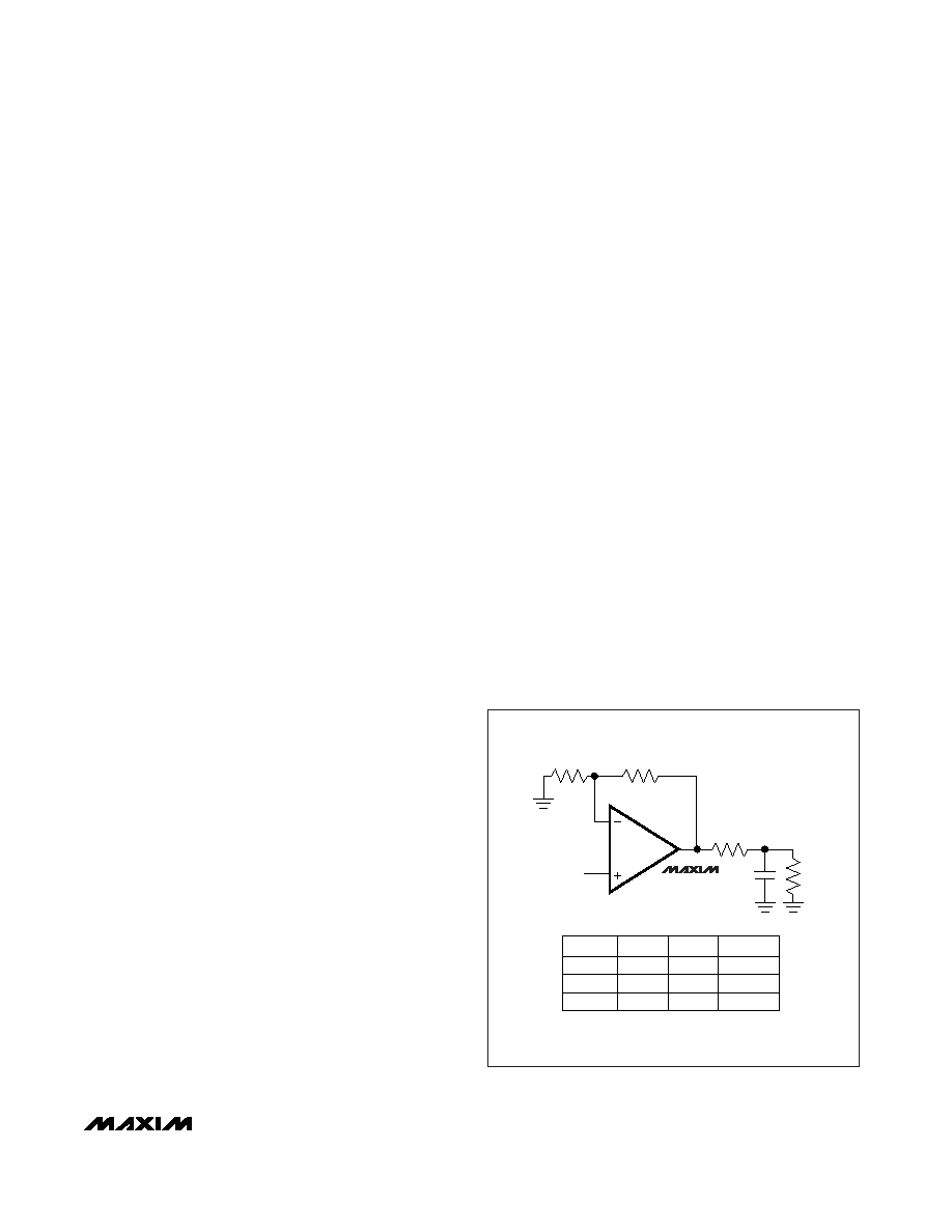
RF
RG
RS*
CL
VIN
PART
MAX4265
MAX4266
MAX4267
RF ()
24
500
RG ()
∞
500
125
GAIN (V/V)
+1
+2
+5
RL
*OPTIONAL, USED TO MINIMIZE PEAKING FOR CL > 15pF.
MAX4265
MAX4266
MAX4267
Figure 1. Noninverting Configuration
相关PDF资料 |
PDF描述 |
|---|---|
| RCWL1210R680JNEA | RES .68 OHM 1/3W 5% 1210 SMD |
| MAX4270EEE | IC OPAMP DUAL 350MHZ 16-QSOP |
| 320551 | CONN #8 RING TERM 16-22 AWG |
| MAX4018ESD+T | IC OP AMP SNGL SPLY R-R 14-SOIC |
| 33459 | CONN RING 10-12 AWG #5/16 SOLIS |
相关代理商/技术参数 |
参数描述 |
|---|---|
| MAX4270ESD-T | 功能描述:高速运算放大器 Single-Supply 200MHz w/Enable RoHS:否 制造商:Texas Instruments 通道数量:1 电压增益 dB:116 dB 输入补偿电压:0.5 mV 转换速度:55 V/us 工作电源电压:36 V 电源电流:7.5 mA 最大工作温度:+ 85 C 安装风格:SMD/SMT 封装 / 箱体:SOIC-8 封装:Tube |
| MAX4271ESA | 功能描述:热插拔功率分布 RoHS:否 制造商:Texas Instruments 产品:Controllers & Switches 电流限制: 电源电压-最大:7 V 电源电压-最小:- 0.3 V 工作温度范围: 功率耗散: 安装风格:SMD/SMT 封装 / 箱体:MSOP-8 封装:Tube |
| MAX4271ESA+ | 功能描述:热插拔功率分布 3-12V Current-Limit Hot Swap Controller RoHS:否 制造商:Texas Instruments 产品:Controllers & Switches 电流限制: 电源电压-最大:7 V 电源电压-最小:- 0.3 V 工作温度范围: 功率耗散: 安装风格:SMD/SMT 封装 / 箱体:MSOP-8 封装:Tube |
| MAX4271ESA+T | 功能描述:热插拔功率分布 3-12V Current-Limit Hot Swap Controller RoHS:否 制造商:Texas Instruments 产品:Controllers & Switches 电流限制: 电源电压-最大:7 V 电源电压-最小:- 0.3 V 工作温度范围: 功率耗散: 安装风格:SMD/SMT 封装 / 箱体:MSOP-8 封装:Tube |
| MAX4271ESA-G05 | 功能描述:热插拔功率分布 RoHS:否 制造商:Texas Instruments 产品:Controllers & Switches 电流限制: 电源电压-最大:7 V 电源电压-最小:- 0.3 V 工作温度范围: 功率耗散: 安装风格:SMD/SMT 封装 / 箱体:MSOP-8 封装:Tube |
发布紧急采购,3分钟左右您将得到回复。