- 您现在的位置:买卖IC网 > PDF目录3337 > MAX4294ESD (Maxim Integrated Products)IC OPAMP 1.8VU R/R I/O 14-SOIC PDF资料下载
参数资料
| 型号: | MAX4294ESD |
| 厂商: | Maxim Integrated Products |
| 文件页数: | 4/18页 |
| 文件大小: | 0K |
| 描述: | IC OPAMP 1.8VU R/R I/O 14-SOIC |
| 产品培训模块: | Lead (SnPb) Finish for COTS Obsolescence Mitigation Program |
| 标准包装: | 50 |
| 放大器类型: | 通用 |
| 电路数: | 4 |
| 输出类型: | 满摆幅 |
| 转换速率: | 0.2 V/µs |
| 增益带宽积: | 500kHz |
| 电流 - 输入偏压: | 15nA |
| 电压 - 输入偏移: | 200µV |
| 电流 - 电源: | 100µA |
| 电流 - 输出 / 通道: | 20mA |
| 电压 - 电源,单路/双路(±): | 1.8 V ~ 5.5 V,±0.9 V ~ 2.75 V |
| 工作温度: | -40°C ~ 85°C |
| 安装类型: | 表面贴装 |
| 封装/外壳: | 14-SOIC(0.154",3.90mm 宽) |
| 供应商设备封装: | 14-SOIC |
| 包装: | 管件 |
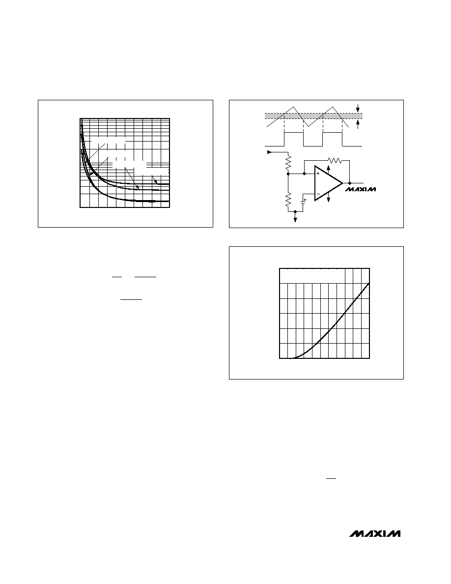
MAX4291/MAX4292/MAX4294 When the output of the comparator is low, the supply
current increases. The output stage has biasing circuit-
ry to monitor the output current. When the amplifier is
used as a comparator, the output stage is overdriven
and the current through the biasing circuitry increases
to maximum. For the MAX4291, typical supply currents
increase to 1.5mA with VCC = 1.8V and to 9mA when
VCC = 5.0V (Figure 10).
Using the MAX4291/MAX4292/MAX4294
as Low-Power Current Monitors
The MAX4291/MAX4292/MAX4294 are ideal for appli-
cations powered from a two-cell battery stack. Figure
11 shows an application circuit in which the MAX4291
is used for monitoring the current of a two-cell battery
stack. In this circuit, a current load is applied, and the
voltage drop at the battery terminal is sensed.
The voltage on the load side of the battery stack is
equal to the voltage at the emitter of Q1 due to the
feedback loop containing the op amp. As the load cur-
rent increases, the voltage drop across R1 and R2
increases. Thus, R2 provides a fraction of the load cur-
rent (set by the ratio of R1 and R2) that flows into the
emitter of the PNP transistor. Neglecting PNP base cur-
rent, this current flows into R3, producing a ground-ref-
erenced voltage proportional to the load current. To
minimize errors, scale R1 to give a voltage drop that is
large enough in comparison to the op amp’s VOS.
Calculate the output voltage of the application using
the following equation:
VI
R1
R2
R3
OUT
LOAD
=×
×
Ultra-Small, 1.8V, Power,
Rail-to-Rail I/O Op Amps
12
______________________________________________________________________________________
060
90
20
30
10
40
50
80
70
100
PROPAGATION DELAY
vs. INPUT OVERDRIVE
VOD (mV)
10
100
1000
t
PD
(
s)
tPD+, VCC = 5.5V
tPD-, VCC = 5.5V
tPD+, VCC = 1.8V
tPD-, VCC = 1.8V
Figure 8. Propagation Delay vs. Input Overdrive
R2
R1
VSIG
OUTPUT
INPUT
VOH
VOL
VEE = GND
VCC
VOUT
RHYST
VEE = GND
MAX4291
MAX4292
MAX4294
HYSTERESIS
VLO
VHI
VREF
Figure 9. Hysteresis Comparator Circuit
0
6
2
4
8
10
12
0
2.0 2.5 3.0
1.0
0.5
1.5
3.5
4.5 5.0
4.0
5.5
MAXIMUM SUPPLY CURRENT PER AMPLIFIER
vs. SUPPLY VOLTAGE
SUPPLY VOLTAGE (V)
MAXIMUM
SUPPLY
CURRENT
(mA)
COMPARATOR CONFIGURATION
VIN+ = (VIN-) - 100mV
Figure 10. Maximum Supply Current per Amplifier vs. Supply
Voltage
V
1
R1
R2
R1
R
V
R1
R
V
HYST
HI
LO
HI
HYST
REF
LO
HI
HYST
CC
=
=+
+
=
相关PDF资料 |
PDF描述 |
|---|---|
| 81080-650201 | CONN HEADER 80POS STR SHORT T |
| 81080-560203-RB | CONN HEADER 80POS R/A LONG T/ |
| N4660-2200 | CONN HEADER 60POS .100 SMD GOLD |
| 3AP 500-R | FUSE 500MA 250V FAST AXL 3AP |
| 81068-660303 | CONN HEADER 68POS STR LONG T/ |
相关代理商/技术参数 |
参数描述 |
|---|---|
| MAX4294ESD+ | 功能描述:运算放大器 - 运放 1.8V uPower Rail-Rail RoHS:否 制造商:STMicroelectronics 通道数量:4 共模抑制比(最小值):63 dB 输入补偿电压:1 mV 输入偏流(最大值):10 pA 工作电源电压:2.7 V to 5.5 V 安装风格:SMD/SMT 封装 / 箱体:QFN-16 转换速度:0.89 V/us 关闭:No 输出电流:55 mA 最大工作温度:+ 125 C 封装:Reel |
| MAX4294ESD+T | 功能描述:运算放大器 - 运放 1.8V uPower Rail-Rail RoHS:否 制造商:STMicroelectronics 通道数量:4 共模抑制比(最小值):63 dB 输入补偿电压:1 mV 输入偏流(最大值):10 pA 工作电源电压:2.7 V to 5.5 V 安装风格:SMD/SMT 封装 / 箱体:QFN-16 转换速度:0.89 V/us 关闭:No 输出电流:55 mA 最大工作温度:+ 125 C 封装:Reel |
| MAX4294ESD-T | 功能描述:运算放大器 - 运放 1.8V uPower Rail-Rail RoHS:否 制造商:STMicroelectronics 通道数量:4 共模抑制比(最小值):63 dB 输入补偿电压:1 mV 输入偏流(最大值):10 pA 工作电源电压:2.7 V to 5.5 V 安装风格:SMD/SMT 封装 / 箱体:QFN-16 转换速度:0.89 V/us 关闭:No 输出电流:55 mA 最大工作温度:+ 125 C 封装:Reel |
| MAX4294EUD | 功能描述:运算放大器 - 运放 1.8V uPower Rail-Rail RoHS:否 制造商:STMicroelectronics 通道数量:4 共模抑制比(最小值):63 dB 输入补偿电压:1 mV 输入偏流(最大值):10 pA 工作电源电压:2.7 V to 5.5 V 安装风格:SMD/SMT 封装 / 箱体:QFN-16 转换速度:0.89 V/us 关闭:No 输出电流:55 mA 最大工作温度:+ 125 C 封装:Reel |
| MAX4294EUD+ | 功能描述:运算放大器 - 运放 1.8V uPower Rail-Rail RoHS:否 制造商:STMicroelectronics 通道数量:4 共模抑制比(最小值):63 dB 输入补偿电压:1 mV 输入偏流(最大值):10 pA 工作电源电压:2.7 V to 5.5 V 安装风格:SMD/SMT 封装 / 箱体:QFN-16 转换速度:0.89 V/us 关闭:No 输出电流:55 mA 最大工作温度:+ 125 C 封装:Reel |
发布紧急采购,3分钟左右您将得到回复。