- 您现在的位置:买卖IC网 > PDF目录9831 > MAX4362ESD+T (Maxim Integrated Products)IC ADSL DRIVER/RX 14-SOIC PDF资料下载
参数资料
| 型号: | MAX4362ESD+T |
| 厂商: | Maxim Integrated Products |
| 文件页数: | 13/13页 |
| 文件大小: | 0K |
| 描述: | IC ADSL DRIVER/RX 14-SOIC |
| 产品培训模块: | Lead (SnPb) Finish for COTS Obsolescence Mitigation Program |
| 标准包装: | 2,500 |
| 类型: | 收发器 |
| 驱动器/接收器数: | 2/2 |
| 规程: | DSL |
| 电源电压: | 4.5 V ~ 5.5 V |
| 安装类型: | 表面贴装 |
| 封装/外壳: | 14-SOIC(0.154",3.90mm 宽) |
| 供应商设备封装: | 14-SOIC |
| 包装: | 带卷 (TR) |
MAX4361/MAX4362/MAX4363
ADSL Drivers/Receivers for Customer Premise
Equipment
_______________________________________________________________________________________
9
Applications Information
Power Supply and Decoupling
The MAX4361/MAX4362/MAX4363 should be powered
from a well-regulated, low-noise, 4.5V to 5.5V supply in
order to optimize the ADSL upstream drive capability to
+12.5dBm and maintain the best SFDR.
High-quality capacitors with low equivalent series resis-
tance (ESR) such as multilayer ceramic capacitors
(MLCCs) should be used to minimize supply voltage
ripple and power dissipation. A larger capacitor located
in proximity to the MAX4361/MAX4362/MAX4363
improves decoupling for lower frequency signals.
In addition, 0.1F MLCC decoupling capacitors should
be located as close as possible to each of the power-
supply pins, no more than 1/8 inch away. An additional
large (4.7F to 10F) tantalum capacitor should be
placed on the board near the supply terminals to sup-
ply current for fast, large-signal changes at the
MAX4361/MAX4362/MAX4363 outputs.
MAX4361/MAX4362
The MAX4361/MAX4362 require a single 0.1F bypass
from V+ to ground located as close as possible to the
IC leads.
MAX4363
The MAX4363 features separate supply and ground
pins for the receiver and driver amplifiers. Bypass the
V+ (RX) supply to the GND (RX) pin with a 0.1F capaci-
tor. Bypass the V+ (TX) supply to the GND (TX) pin with
a separate 0.1F capacitor. Both capacitors should be
placed as close as possible to their respective IC leads.
USB Applications
The 5V supplied at the universal serial bus (USB) port
may be poorly regulated or unable to supply the peak
currents required by an ADSL modem. Improving the
quality of the supply will optimize the performance of
the MAX4361/MAX4362/MAX4363 in a USB-supplied
CPE ADSL modem. This can be accomplished through
the use of a step-up DC-to-DC converter or switching
power supply followed by a low-dropout (LDO) regula-
tor. Careful attention must be paid to decoupling the
power supply at the output of the DC-to-DC converter,
the output of the LDO regulator and the supply pins of
the MAX4361/MAX4362/MAX4363.
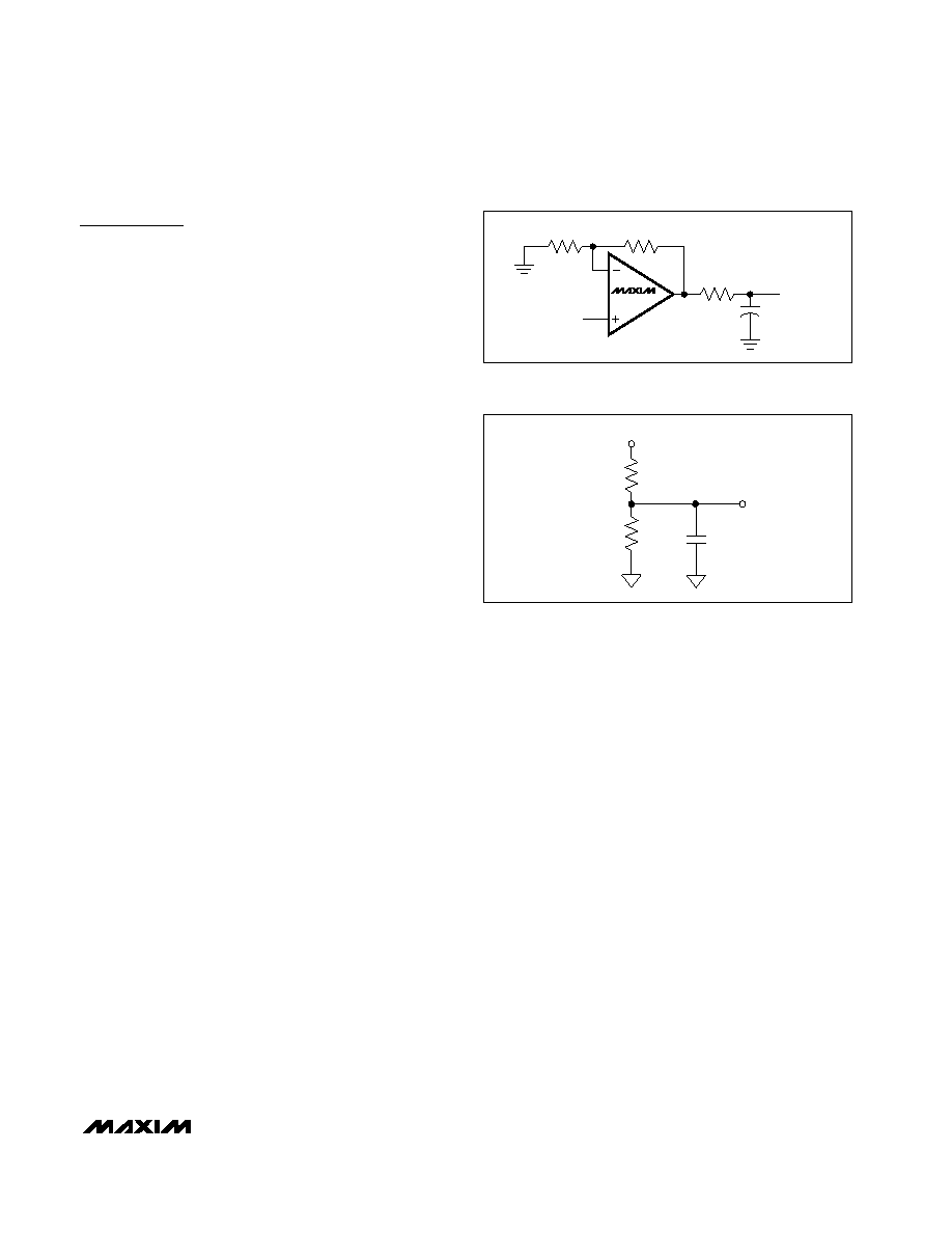
Driving a Capacitive Load
The MAX4361/MAX4362/MAX4363 are capable of dri-
ving capacitive loads up to 2nF. Most hybrid circuits
are well under this limit. For additional capacitive-drive
capability use isolation resistors between the output
and the load to reduce ringing on the output signal. In a
typical hybrid the back-matching resistors provide suffi-
cient isolation for most any capacitive-loading condition
(see Figure 1).
Method for Generating a Midsupply
Voltage
To operate an amplifier on a single-voltage supply, a
voltage midway between the supply and ground must be
generated to properly bias the inputs and the outputs.
A voltage divider can be created with two equal-value
resistors (Figure 2). There is a trade-off between the
power consumed by the divider and the voltage drop
across these resistors due to the positive input bias
currents. Selecting 2.7k
for R1 and R2 will create a
voltage divider that draws less than 1mA from a 5V
supply. Use a decoupling capacitor (0.1F) at the node
where VREF is generated.
Power Dissipation
It is important to consider the total power dissipation of
the MAX4361/MAX4362/MAX4363 in order to properly
size the heat sink area of an application. With some
simplifying assumptions we can estimate the total
power dissipated in the driver (see Typical Operating
Figure 2. Voltage-Divider Reference
Figure 1. Driving Capacitive Load
1k
500
3.1
CLOAD
OUTPUT
INPUT
MAX436 _
R1
2.7k
R2
2.7k
0.1
F
VREF
5V
相关PDF资料 |
PDF描述 |
|---|---|
| VE-250-MX-F4 | CONVERTER MOD DC/DC 5V 75W |
| MS27656E23F55S | CONN RCPT 55POS WALL MNT W/SCKT |
| VE-J60-MX-F3 | CONVERTER MOD DC/DC 5V 75W |
| MAX4362EUB+T | IC DRVR/RX ADSL 10-UMAX |
| MX7572LCWG12+ | IC ADC 12BIT HS 24-SOIC |
相关代理商/技术参数 |
参数描述 |
|---|---|
| MAX4362EUB | 功能描述:高速运算放大器 ADSL Driver/Receiver RoHS:否 制造商:Texas Instruments 通道数量:1 电压增益 dB:116 dB 输入补偿电压:0.5 mV 转换速度:55 V/us 工作电源电压:36 V 电源电流:7.5 mA 最大工作温度:+ 85 C 安装风格:SMD/SMT 封装 / 箱体:SOIC-8 封装:Tube |
| MAX4362EUB+ | 功能描述:高速运算放大器 ADSL Driver/Receiver RoHS:否 制造商:Texas Instruments 通道数量:1 电压增益 dB:116 dB 输入补偿电压:0.5 mV 转换速度:55 V/us 工作电源电压:36 V 电源电流:7.5 mA 最大工作温度:+ 85 C 安装风格:SMD/SMT 封装 / 箱体:SOIC-8 封装:Tube |
| MAX4362EUB+T | 功能描述:高速运算放大器 ADSL Driver/Receiver RoHS:否 制造商:Texas Instruments 通道数量:1 电压增益 dB:116 dB 输入补偿电压:0.5 mV 转换速度:55 V/us 工作电源电压:36 V 电源电流:7.5 mA 最大工作温度:+ 85 C 安装风格:SMD/SMT 封装 / 箱体:SOIC-8 封装:Tube |
| MAX4362EUB-T | 功能描述:高速运算放大器 ADSL Driver/Receiver RoHS:否 制造商:Texas Instruments 通道数量:1 电压增益 dB:116 dB 输入补偿电压:0.5 mV 转换速度:55 V/us 工作电源电压:36 V 电源电流:7.5 mA 最大工作温度:+ 85 C 安装风格:SMD/SMT 封装 / 箱体:SOIC-8 封装:Tube |
| MAX4363ESP | 功能描述:高速运算放大器 RoHS:否 制造商:Texas Instruments 通道数量:1 电压增益 dB:116 dB 输入补偿电压:0.5 mV 转换速度:55 V/us 工作电源电压:36 V 电源电流:7.5 mA 最大工作温度:+ 85 C 安装风格:SMD/SMT 封装 / 箱体:SOIC-8 封装:Tube |
发布紧急采购,3分钟左右您将得到回复。