参数资料
| 型号: | MAX4382ESD+ |
| 厂商: | Maxim Integrated Products |
| 文件页数: | 3/16页 |
| 文件大小: | 0K |
| 描述: | IC OP AMP R-R SS 14-SOIC |
| 产品培训模块: | Lead (SnPb) Finish for COTS Obsolescence Mitigation Program |
| 标准包装: | 50 |
| 放大器类型: | 电压反馈 |
| 电路数: | 3 |
| 输出类型: | 满摆幅 |
| 转换速率: | 485 V/µs |
| -3db带宽: | 210MHz |
| 电流 - 输入偏压: | 8.5µA |
| 电压 - 输入偏移: | 3000µV |
| 电流 - 电源: | 7.5mA |
| 电流 - 输出 / 通道: | 75mA |
| 电压 - 电源,单路/双路(±): | 4.5 V ~ 11 V,±2.25 V ~ 5.5 V |
| 工作温度: | -40°C ~ 85°C |
| 安装类型: | 表面贴装 |
| 封装/外壳: | 14-SOIC(0.154",3.90mm 宽) |
| 供应商设备封装: | 14-SOIC |
| 包装: | 管件 |
| 产品目录页面: | 1389 (CN2011-ZH PDF) |
MAX4380–MAX4384
Ultra-Small, Low-Cost, 210MHz, Single-Supply
Op Amps with Rail-to-Rail Outputs and Disable
______________________________________________________________________________________
11
have a 16ns settling time to 0.1%, 485V/s slew rates,
and output-current-drive capability of up to 75mA
making them ideal for driving video loads.
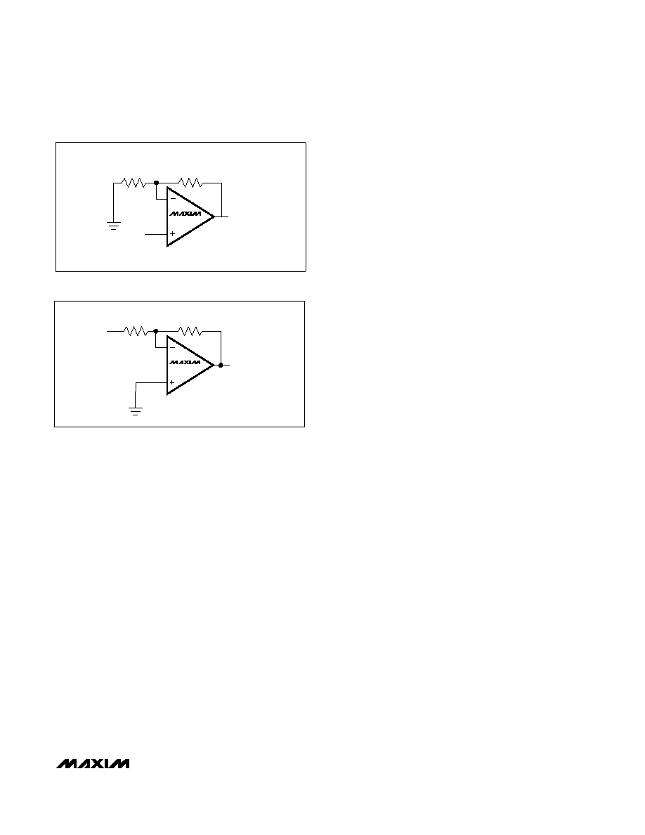
Inverting and Noninverting Configurations
Select the gain-setting feedback (RF) and input (RG)
resistor values to fit your application. Large resistor val-
ues increase voltage noise and interact with the ampli-
fier’s input and PC board capacitance. This can
generate undesirable poles and zeros and decrease
bandwidth or cause oscillations. For example, a nonin-
verting gain-of-two configuration (RF = RG) using 1k
resistors, combined with 1pF of amplifier input capaci-
tance and 1pF of PC board capacitance, causes a
pole at 159MHz. Since this pole is within the amplifier
bandwidth, it jeopardizes stability. Reducing the 1k
resistors to 100
extends the pole frequency to
1.59GHz, but could limit output swing by adding 200
in parallel with the amplifier’s load resistor
(Figures 1a and 1b).
Layout and Power-Supply Bypassing
These amplifiers operate from a single +4.5V to +11V
power supply or from dual ±2.25V to ±5.5V supplies. For
single-supply operation, bypass VCC to ground with a
0.1F capacitor as close to the pin as possible. If operat-
ing with dual supplies, bypass each supply with a 0.1F
capacitor.
Maxim recommends using microstrip and stripline
techniques to obtain full bandwidth. To ensure that the
PC board does not degrade the amplifier’s perfor-
mance, design it for a frequency greater than 1GHz.
Pay careful attention to inputs and outputs to avoid
large parasitic capacitance. Whether or not you use a
constant-impedance board, observe the following
design guidelines:
Don’t use wire-wrap boards; they are too inductive.
Don’t use IC sockets; they increase parasitic capaci-
tance and inductance.
Use surface-mount instead of through-hole compo-
nents for better high-frequency performance.
Use a PC board with at least two layers; it should be
as free from voids as possible.
Keep signal lines as short and as straight as possi-
ble. Do not make 90° turns; round all corners.
Rail-to-Rail Outputs,
Ground-Sensing Inputs
For +5V single-supply operation, the input common-
mode range extends from (VEE - 200mV) to (VCC
- 2.25V) with excellent common-mode rejection.
Beyond this range, the amplifier output is a nonlinear
function of the input, but does not undergo phase
reversal or latchup.
For ±5V dual-supply operation, the common-mode
range is from VEE to (VCC - 2.25V)
For +5V single-supply operation the output swings to
within 50mV of either power-supply rail with a 2k
load. The input ground sensing and the rail-to-rail out-
put substantially increase the dynamic range. With a
symmetric input in a single +5V application, the input
can swing 2.95Vp-p and the output can swing 4.9Vp-p
with minimal distortion.
Low-Power Disable Mode
The disable feature (DISABLE_) allows the amplifier to
be placed in a low-power, high-output-impedance
state. When the disable pin (DISABLE_) is active, the
amplifier’s output impedance is 35k
. This high resis-
tance and the low 2pF output capacitance make the
MAX4380–MAX4382 and the MAX4384 ideal in
RF/video multiplexer or switch applications. For larger
arrays, pay careful attention to capacitive loading.
Refer to the Output Capacitive Loading and Stability
section.
IN
RG
VOUT = -(RF / RG) VIN
RF
VOUT
MAX438 _
Figure 1b. Inverting Gain Configuration
IN
RG
VOUT = [1+ (RF / RG)] VIN
RF
VOUT
MAX438 _
Figure 1a. Noninverting Gain Configuration
相关PDF资料 |
PDF描述 |
|---|---|
| PCF0805R-127KBT1 | RES 127K OHM 0.1W 0805 0.1% SMD |
| 3-87230-0 | CONN HEADER RT/A 60POS .100 15AU |
| 170M3188 | FUSE 50A 1250V 1TN/110 AR CU |
| MAX4382EEE+ | IC OP AMP R-R SS 16-QSOP |
| 69916-001 | .500 VERT HDR W/O MTG HO-LES |
相关代理商/技术参数 |
参数描述 |
|---|---|
| MAX4382ESD+ | 功能描述:高速运算放大器 210MHz Single-Supply w/Rail-Rail Out RoHS:否 制造商:Texas Instruments 通道数量:1 电压增益 dB:116 dB 输入补偿电压:0.5 mV 转换速度:55 V/us 工作电源电压:36 V 电源电流:7.5 mA 最大工作温度:+ 85 C 安装风格:SMD/SMT 封装 / 箱体:SOIC-8 封装:Tube |
| MAX4382ESD+T | 功能描述:高速运算放大器 210MHz Single-Supply w/Rail-Rail Out RoHS:否 制造商:Texas Instruments 通道数量:1 电压增益 dB:116 dB 输入补偿电压:0.5 mV 转换速度:55 V/us 工作电源电压:36 V 电源电流:7.5 mA 最大工作温度:+ 85 C 安装风格:SMD/SMT 封装 / 箱体:SOIC-8 封装:Tube |
| MAX4382ESD-T | 功能描述:高速运算放大器 RoHS:否 制造商:Texas Instruments 通道数量:1 电压增益 dB:116 dB 输入补偿电压:0.5 mV 转换速度:55 V/us 工作电源电压:36 V 电源电流:7.5 mA 最大工作温度:+ 85 C 安装风格:SMD/SMT 封装 / 箱体:SOIC-8 封装:Tube |
| MAX4382EUD | 功能描述:高速运算放大器 RoHS:否 制造商:Texas Instruments 通道数量:1 电压增益 dB:116 dB 输入补偿电压:0.5 mV 转换速度:55 V/us 工作电源电压:36 V 电源电流:7.5 mA 最大工作温度:+ 85 C 安装风格:SMD/SMT 封装 / 箱体:SOIC-8 封装:Tube |
| MAX4382EUD+ | 功能描述:高速运算放大器 210MHz Single-Supply w/Rail-Rail Out RoHS:否 制造商:Texas Instruments 通道数量:1 电压增益 dB:116 dB 输入补偿电压:0.5 mV 转换速度:55 V/us 工作电源电压:36 V 电源电流:7.5 mA 最大工作温度:+ 85 C 安装风格:SMD/SMT 封装 / 箱体:SOIC-8 封装:Tube |
发布紧急采购,3分钟左右您将得到回复。