参数资料
| 型号: | MAX4389EUT+T |
| 厂商: | Maxim Integrated Products |
| 文件页数: | 12/24页 |
| 文件大小: | 0K |
| 描述: | IC OP AMP R-R SOT23-6 |
| 产品培训模块: | Lead (SnPb) Finish for COTS Obsolescence Mitigation Program |
| 标准包装: | 1 |
| 应用: | 电压反馈 |
| 输出类型: | 满摆幅 |
| 电路数: | 1 |
| -3db带宽: | 85MHz |
| 转换速率: | 500 V/µs |
| 电流 - 电源: | 6mA |
| 电流 - 输出 / 通道: | 95mA |
| 电压 - 电源,单路/双路(±): | 4.5 V ~ 11 V,±2.25 V ~ 5.5 V |
| 安装类型: | 表面贴装 |
| 封装/外壳: | SOT-23-6 |
| 供应商设备封装: | SOT-6 |
| 包装: | 标准包装 |
| 产品目录页面: | 1389 (CN2011-ZH PDF) |
| 其它名称: | MAX4389EUT+TDKR |
MAX4389/MAX4390/MAX4392–MAX4396
Ultra-Small, Low-Cost, 85MHz Op Amps with
Rail-to-Rail Outputs and Disable
2
_______________________________________________________________________________________
ABSOLUTE MAXIMUM RATINGS
Stresses beyond those listed under “Absolute Maximum Ratings” may cause permanent damage to the device. These are stress ratings only, and functional
operation of the device at these or any other conditions beyond those indicated in the operational sections of the specifications is not implied. Exposure to
absolute maximum rating conditions for extended periods may affect device reliability.
Supply Voltage (VCC to VEE) ..................................-0.3V to +12V
IN_+, IN_-, OUT_,
DISABLE.............(VEE - 0.3V) to (VCC + 0.3V)
Differential Input Voltage ....................................................±2.5V
Current into Input Pins ......................................................±20mA
Output Short-Circuit Duration to
VCC or VEE (Note 1)................................................Continuous
Continuous Power Dissipation (TA = +70°C)
5-Pin SOT23 (derate 7.1mW/°C above +70°C)............571mW
6-Pin SOT23 (derate 8.7mW/°C above +70°C)............696mW
6-Pin SC70 (derate 3.1mW/°C above +70°C) ..............245mW
8-Pin SO (derate 5.88mW/°C above +70°C)................471mW
8-Pin MAX (derate 4.5mW/°C above +70°C) .............362mW
10-Pin MAX (derate 5.6mW/°C above +70°C) ...........444mW
14-Pin SO (derate 8.33mW/°C above +70°C)..............667mW
14-Pin TSSOP (derate 10mW/°C above +70°C) ..........727mW
20-Pin TSSOP (derate 10.9mW/°C above +70°C) .......879mW
Operating Temperature Range ...........................-40°C to +85°C
Junction Temperature ......................................................+150°C
Storage Temperature Range .............................-65°C to +150°C
Lead Temperature (soldering, 10s) .................................+300°C
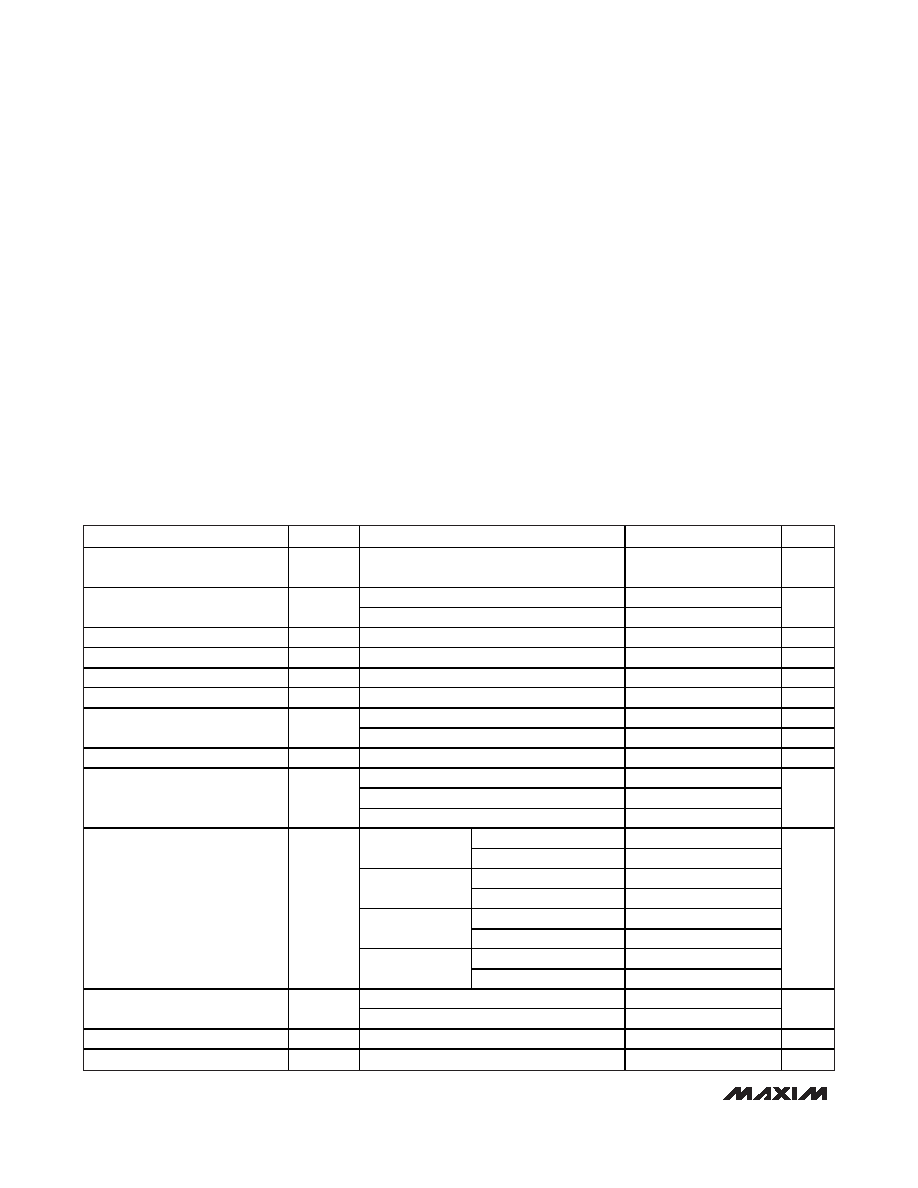
DC ELECTRICAL CHARACTERISTICS—Single Supply
(VCC = 5V, VEE = 0V, VCM = VCC/2, VOUT = VCC/2, RL = ∞ to VCC/2, DISABLE_ = VCC (MAX4389/MAX4393/MAX4394/MAX4396),
TA = TMIN to TMAX, unless otherwise noted. Typical values are at TA = +25°C.) (Note 2)
PARAMETER
SYMBOL
CONDITIONS
MIN
TYP
MAX
UNITS
Input Common-Mode Voltage
Range
VCM
Guaranteed by CMRR test
VEE -
0.2
VCC -
2.25
V
TA = +25°C
5
18
Input Offset Voltage
VOS
TA = -40°C to +85°C
26
mV
Input Offset Voltage Matching
MAX4392–MAX4396
1
mV
Input Offset Voltage Tempco
TCVOS
15
V/°C
Input Bias Current
IB
2.5
15
A
Input Offset Current
IOS
0.2
5
A
Differential mode (-1V
≤ VIN ≤ +1V)
70
k
Ω
Input Resistance
RIN
Common mode (-0.2V
≤ VCM ≤ +2.75V)
3
M
Ω
Common-Mode Rejection Ratio
CMRR
(VEE - 0.2V)
≤ VCM ≤ (VCC - 2.25V)
70
95
dB
0.25V
≤ VOUT ≤ 4.75V, RL = 2kΩ
50
70
0.8V
≤ VOUT ≤ 4.5V, RL = 150Ω
50
60
Open-Loop Gain
AVOL
1V
≤ VOUT ≤ 4V, RL = 50Ω
58
dB
VCC - VOH
0.065
0.25
RL = 2k
Ω
VOL - VEE
0.05
0.15
VCC - VOH
0.3
0.5
RL = 150
Ω
VOL - VEE
0.25
0.5
VCC - VOH
0.5
0.8
RL = 75
Ω
VOL - VEE
0.45
0.8
VCC - VOH
1
1.7
Output Voltage Swing
VOUT
RL = 75
Ω to
ground
VOL - VEE
0.025
0.1
V
Sinking from RL = 75
Ω to VCC
40
55
Output Current
IOUT
Sourcing into RL = 75
Ω to VEE
40
50
mA
Output Short-Circuit Current
ISC
Sinking or sourcing
±100
mA
Open-Loop Output Resistance
ROUT
8
Ω
Note 1: Continuous power dissipation must also be observed.
相关PDF资料 |
PDF描述 |
|---|---|
| MAX9542AEE+T | IC AMP VIDEO MUX 2:1 16-QSOP |
| VI-23M-IV-F4 | CONVERTER MOD DC/DC 10V 150W |
| VI-B5K-MU | CONVERTER MOD DC/DC 40V 200W |
| VI-23L-IV-F3 | CONVERTER MOD DC/DC 28V 150W |
| VI-B5J-MU | CONVERTER MOD DC/DC 36V 200W |
相关代理商/技术参数 |
参数描述 |
|---|---|
| MAX4389EXT | 制造商:Maxim Integrated Products 功能描述:- Rail/Tube |
| MAX4389EXT/V+T | 功能描述:高速运算放大器 85MHz w/Rail-Rail Output RoHS:否 制造商:Texas Instruments 通道数量:1 电压增益 dB:116 dB 输入补偿电压:0.5 mV 转换速度:55 V/us 工作电源电压:36 V 电源电流:7.5 mA 最大工作温度:+ 85 C 安装风格:SMD/SMT 封装 / 箱体:SOIC-8 封装:Tube |
| MAX4389EXT+ | 制造商:Maxim Integrated Products 功能描述:OP AMP SGL VOLT FDBK R-R O/P 5.5V/11V 6PIN SC-70 - Rail/Tube |
| MAX4389EXT+T | 功能描述:高速运算放大器 85MHz w/Rail-Rail Output RoHS:否 制造商:Texas Instruments 通道数量:1 电压增益 dB:116 dB 输入补偿电压:0.5 mV 转换速度:55 V/us 工作电源电压:36 V 电源电流:7.5 mA 最大工作温度:+ 85 C 安装风格:SMD/SMT 封装 / 箱体:SOIC-8 封装:Tube |
| MAX4389EXT-T | 功能描述:运算放大器 - 运放 RoHS:否 制造商:STMicroelectronics 通道数量:4 共模抑制比(最小值):63 dB 输入补偿电压:1 mV 输入偏流(最大值):10 pA 工作电源电压:2.7 V to 5.5 V 安装风格:SMD/SMT 封装 / 箱体:QFN-16 转换速度:0.89 V/us 关闭:No 输出电流:55 mA 最大工作温度:+ 125 C 封装:Reel |
发布紧急采购,3分钟左右您将得到回复。