- 您现在的位置:买卖IC网 > PDF目录10346 > MAX4411ETP+T (Maxim Integrated Products)IC AMP AUDIO .08W STER AB 20TQFN PDF资料下载
参数资料
| 型号: | MAX4411ETP+T |
| 厂商: | Maxim Integrated Products |
| 文件页数: | 4/18页 |
| 文件大小: | 0K |
| 描述: | IC AMP AUDIO .08W STER AB 20TQFN |
| 产品培训模块: | Lead (SnPb) Finish for COTS Obsolescence Mitigation Program |
| 标准包装: | 2,500 |
| 系列: | DirectDrive® |
| 类型: | AB 类 |
| 输出类型: | 耳机,2-通道(立体声) |
| 在某负载时最大输出功率 x 通道数量: | 80mW x 2 @ 16 欧姆 |
| 电源电压: | 1.8 V ~ 3.6 V |
| 特点: | 消除爆音,短路保护和热保护,关闭 |
| 安装类型: | 表面贴装 |
| 供应商设备封装: | 20-TQFN-EP(4x4) |
| 封装/外壳: | 20-WFQFN 裸露焊盘 |
| 包装: | 带卷 (TR) |
MAX4411
80mW, Fixed-Gain, DirectDrive, Stereo
Headphone Amplifier with Shutdown
12
______________________________________________________________________________________
output, supply, and ground traces improve the maxi-
mum power dissipation in the package.
Thermal-overload protection limits total power dissipa-
tion in the MAX4411. When the junction temperature
exceeds +140°C, the thermal protection circuitry dis-
ables the amplifier output stage. The amplifiers are
enabled once the junction temperature cools by 15°C.
This results in a pulsing output under continuous thermal-
overload conditions.
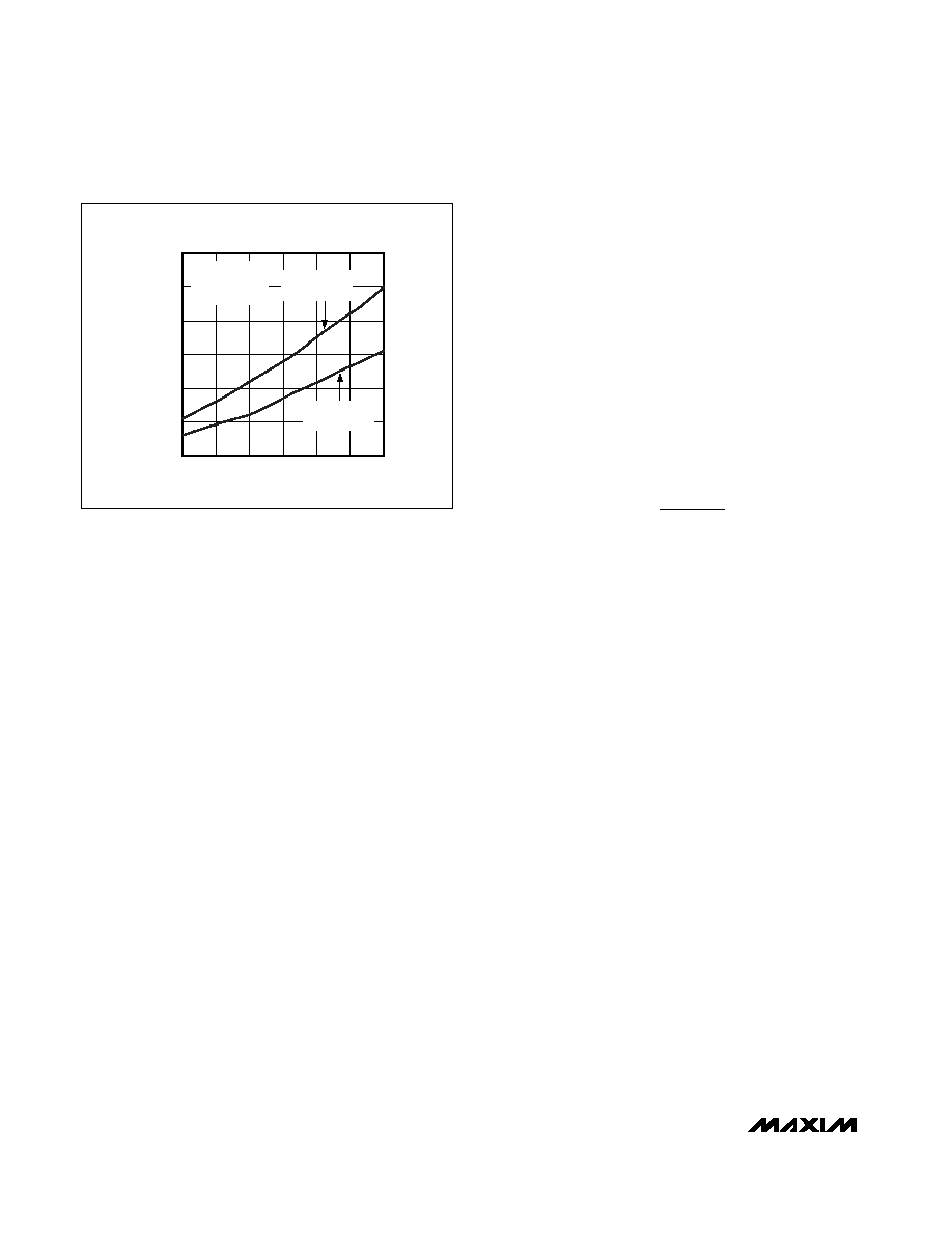
Output Power
The device has been specified for the worst-case sce-
nario—when both inputs are in phase. Under this con-
dition, the drivers simultaneously draw current from the
charge pump, leading to a slight loss in headroom of
VSS. In typical stereo audio applications, the left and
right signals have differences in both magnitude and
phase, subsequently leading to an increase in the max-
imum attainable output power. Figure 5 shows the two
extreme cases for in and out of phase. In reality, the
available power lies between these extremes.
Powering Other Circuits from a
Negative Supply
An additional benefit of the MAX4411 is the internally
generated, negative supply voltage (PVSS). This volt-
age provides the ground-referenced output level. PVSS
can, however, also be used to power other devices
within a design limit current drawn from PVSS to 5mA;
exceeding this affects the headphone driver operation.
A typical application is a negative supply to adjust the
contrast of LCD modules.
PVSS is roughly proportional to PVDD and is not a regu-
lated voltage. The charge-pump output impedance
must be taken into account when powering other
devices from PVSS. The charge-pump output imped-
ance plot appears in the Typical Operating
Characteristics. For best results, use 2.2F charge-
pump capacitors.
Component Selection
Input Filtering
The input capacitor (CIN), in conjunction with the inter-
nal RIN, forms a highpass filter that removes the DC
bias from an incoming signal (see Typical Application
Circuit). The AC-coupling capacitor allows the amplifier
to bias the signal to an optimum DC level. Assuming
zero-source impedance, the -3dB point of the highpass
filter is given by:
RIN is the amplifier’s internal input resistance value
given in the Electrical Characteristics. Choose the CIN
such that f-3dB is well below the lowest frequency of
interest. Setting f-3dB too high affects the amplifier’s low-
frequency response. Use capacitors whose dielectrics
have low-voltage coefficients, such as tantalum or
aluminum electrolytic ones. Capacitors with high-voltage
coefficients, such as ceramics, may result in increased
distortion at low frequencies.
Charge-Pump Capacitor Selection
Use capacitors with an ESR less than 100m
Ω for opti-
mum performance. Low-ESR ceramic capacitors mini-
mize the output resistance of the charge pump. For best
performance over the extended temperature range,
select capacitors with an X7R dielectric. Table 1 lists sug-
gested manufacturers.
Flying Capacitor (C1)
The value of the flying capacitor (C1) affects the charge
pump’s load regulation and output resistance. A C1
value that is too small degrades the device’s ability to
provide sufficient current drive, which leads to a loss of
output voltage. Increasing the value of C1 improves
load regulation and reduces the charge-pump output
resistance to an extent. See the Output Power vs.
Charge-Pump Capacitance and Load Resistance
graph in the Typical Operating Characteristics. Above
2.2F, the on-resistance of the switches and the ESR of
C1 and C2 dominate.
Hold Capacitor (C2)
The hold capacitor value and ESR directly affect the
ripple at PVSS. Increasing the value of C2 reduces
f
RC
dB
IN IN
=
3
1
2
π
OUTPUT POWER vs. SUPPLY VOLTAGE
MAX4411
fig05
SUPPLY VOLTAGE (V)
OUTPUT
POWER
(mW)
3.3
3.0
2.7
2.4
2.1
50
100
150
200
250
300
0
1.8
3.6
fIN = 1kHz
RL = 16
Ω
THD+N = 10%
INPUTS
IN PHASE
INPUTS 180
°
OUT OF PHASE
Figure 5. Output Power vs. Supply Voltage with Inputs In/Out of
Phase
相关PDF资料 |
PDF描述 |
|---|---|
| MS3100A20-19S | CONN RCPT 3POS WALL MNT W/SCKT |
| MS27468T15B19P | CONN RCPT 19POS JAM NUT W/PINS |
| MAX9722AEUE+T | IC AMP AUDIO .13W STER 16TSSOP |
| VI-J02-MX | CONVERTER MOD DC/DC 15V 75W |
| MS27656T11B35SB | CONN RCPT 13POS WALL MNT W/SCKT |
相关代理商/技术参数 |
参数描述 |
|---|---|
| MAX4411EVKIT | 功能描述:音频 IC 开发工具 MAX4411 Eval Kit RoHS:否 制造商:Texas Instruments 产品:Evaluation Kits 类型:Audio Amplifiers 工具用于评估:TAS5614L 工作电源电压:12 V to 38 V |
| MAX4412ESA+ | 功能描述:运算放大器 - 运放 Low-Cost Low-Power Ultra-Small 3V/5V 500MHz Single-Supply Op Amps with Rail-to-Rail Outputs RoHS:否 制造商:STMicroelectronics 通道数量:4 共模抑制比(最小值):63 dB 输入补偿电压:1 mV 输入偏流(最大值):10 pA 工作电源电压:2.7 V to 5.5 V 安装风格:SMD/SMT 封装 / 箱体:QFN-16 转换速度:0.89 V/us 关闭:No 输出电流:55 mA 最大工作温度:+ 125 C 封装:Reel |
| MAX4412ESA+T | 功能描述:运算放大器 - 运放 Single Low-Cost low-Power Ultra-Small 3V/5V 500MHz Single-Supply OP RoHS:否 制造商:STMicroelectronics 通道数量:4 共模抑制比(最小值):63 dB 输入补偿电压:1 mV 输入偏流(最大值):10 pA 工作电源电压:2.7 V to 5.5 V 安装风格:SMD/SMT 封装 / 箱体:QFN-16 转换速度:0.89 V/us 关闭:No 输出电流:55 mA 最大工作温度:+ 125 C 封装:Reel |
| MAX4412EUK | 制造商:Maxim Integrated Products 功能描述:SINGLE, LOW-COST, LOW-POWER, ULTRA-SMALL, 3V/ - Cut Tape Product |
| MAX4412EUK+ | 制造商:Maxim Integrated Products 功能描述:OP AMP SGL VOLT FDBK R-R O/P 5.5V 5PIN SOT-23 - Bulk |
发布紧急采购,3分钟左右您将得到回复。