- 您现在的位置:买卖IC网 > PDF目录2158 > MAX4451ESA+T (Maxim Integrated Products)IC OP AMP R-R DUAL 210MHZ 8-SOIC PDF资料下载
参数资料
| 型号: | MAX4451ESA+T |
| 厂商: | Maxim Integrated Products |
| 文件页数: | 8/15页 |
| 文件大小: | 0K |
| 描述: | IC OP AMP R-R DUAL 210MHZ 8-SOIC |
| 产品培训模块: | Lead (SnPb) Finish for COTS Obsolescence Mitigation Program |
| 标准包装: | 2,500 |
| 放大器类型: | 电压反馈 |
| 电路数: | 2 |
| 输出类型: | 满摆幅 |
| 转换速率: | 485 V/µs |
| -3db带宽: | 210MHz |
| 电流 - 输入偏压: | 6.5µA |
| 电压 - 输入偏移: | 4000µV |
| 电流 - 电源: | 6.5mA |
| 电流 - 输出 / 通道: | 70mA |
| 电压 - 电源,单路/双路(±): | 4.5 V ~ 11 V,±2.25 V ~ 5.5 V |
| 工作温度: | -40°C ~ 85°C |
| 安装类型: | 表面贴装 |
| 封装/外壳: | 8-SOIC(0.154",3.90mm 宽) |
| 供应商设备封装: | 8-SOIC |
| 包装: | 带卷 (TR) |
MAX4450/MAX4451
Ultra-Small, Low-Cost, 210MHz, Single-Supply
Op Amps with Rail-to-Rail Outputs
2
_______________________________________________________________________________________
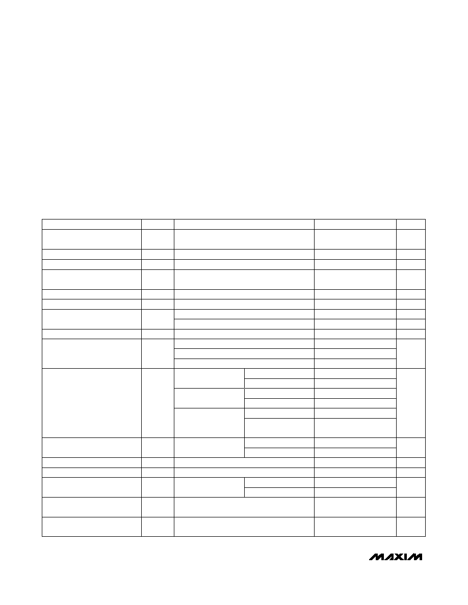
ABSOLUTE MAXIMUM RATINGS
DC ELECTRICAL CHARACTERISTICS
(VCC = +5V, VEE = 0V, RL =
∞ to VCC/2, VOUT = VCC/2, TA = TMIN to TMAX, unless otherwise noted. Typical values are at TA = +25°C.)
(Note 1)
Supply Voltage (VCC to VEE)................................................+12V
IN_-, IN_+, OUT_..............................(VEE - 0.3V) to (VCC + 0.3V)
Output Short-Circuit Current to VCC or VEE ......................150mA
Continuous Power Dissipation (TA = +70°C)
5-Pin SC70-5 (derate 2.5mW/°C above +70°C) ..........200mW
5-Pin SOT23-5 (derate 7.1mW/°C above +70°C) ........571mW
8-Pin SOT23-8 (derate 5.26mW/°C above +70°C) ......421mW
8-Pin SO (derate 5.9mW/°C above +70°C) .................471mW
Operating Temperature Range ...........................-40°C to +85°C
Storage Temperature Range .............................-65°C to +150°C
Lead Temperature (soldering, 10s) .................................+300°C
Stresses beyond those listed under “Absolute Maximum Ratings” may cause permanent damage to the device. These are stress ratings only, and functional
operation of the device at these or at any other conditions beyond those indicated in the operational sections of the specifications is not implied. Exposure
to absolute maximum rating conditions for extended periods may affect device reliability.
PARAMETER
SYMBOL
CONDITIONS
MIN
TYP
MAX
UNITS
V
VEE -VCC
0.20
2.25
Guaranteed by CMRR test
VCM
Input Common-Mode
Voltage Range
Input Offset Voltage (Note 2)
Input Offset Voltage Matching
VOS
426
1.0
mV
V/°C
8
TCVOS
Input Offset Voltage
Temperature Coefficient
Input Bias Current
Input Offset Current
IB
IOS
(Note 2)
6.5
20
0.5
4
A
k
Ω
70
Differential mode (-1V
≤ VIN ≤ +1V)
RIN
Input Resistance
Common mode (-0.2V
≤ VCM ≤ +2.75V)
3
M
Ω
dB
70
95
50
60
48
58
57
dB
V
0.05
0.20
0.05
0.15
0.30
0.50
0.25
0.80
0.5
0.80
0.5
1.75
45
70
mA
Ω
8
±120
46
62
dB
V
54
69
4.5
11.0
6.5
9.0
mA
VCC to VEE
VEE = -5V, VCM = 0V
VEE = 0V, VCM = 2V
VCC = 5V
Sinking or sourcing
VOL - VEE
VCC - VOH
VOL - VEE
VCC - VOH
VOL - VEE
VCC - VOH
1V
≤ VOUT ≤ 4V, RL = 50Ω
0.5V
≤ VOUT ≤ 4.5V, RL = 150Ω
0.25V
≤ VOUT ≤ 4.75V, RL = 2kΩ
(VEE - 0.2V)
≤ VCM ≤ (VCC - 2.25V)
RL = 2k
Ω
RL = 150
Ω
RL = 75
Ω
IS
VS
PSRR
ROUT
ISC
IOUT
VOUT
AVOL
CMRR
Common-Mode Rejection Ratio
Open-Loop Gain (Note 2)
Output Voltage Swing
(Note 2)
Output Current
Output Short-Circuit Current
Open-Loop Output Resistance
Power-Supply Rejection Ratio
(Note 3)
Operating Supply-Voltage
Range
Quiescent Supply Current
(per amplifier)
RL = 50
Ω
25
50
Sourcing
Sinking
相关PDF资料 |
PDF描述 |
|---|---|
| MAX4454ESD+T | IC OPAMP SNGL R-R OUT 14-SOIC |
| MAX4460EUT#TG16 | IC INSTR AMP SGL R-R SOT-23-6 |
| MAX4472EUD+T | IC OP AMP QUAD R-R 9KHZ 14-TSSOP |
| MAX4475AUT#TG16 | IC OP AMP R-R LN 10MHZ SOT23-6 |
| MAX4483AUD+ | IC OP AMP GP QUAD R-R 14-TSSOP |
相关代理商/技术参数 |
参数描述 |
|---|---|
| MAX4452ESA | 制造商:Maxim Integrated Products 功能描述:SC70, LOW-COST, ULTRA-LOW-POWER, +3V/+5V, 200 - Rail/Tube |
| MAX4452ESA+ | 制造商:Maxim Integrated Products 功能描述:OP AMP SGL GP R-R O/P 5.25V 8SOIC N - Rail/Tube |
| MAX4452ESA+T | 制造商:Maxim Integrated Products 功能描述:OP AMP SGL GP R-R O/P 5.25V 8SOIC N - Tape and Reel |
| MAX4452ESA-T | 制造商:Maxim Integrated Products 功能描述:SC70, LOW-COST, ULTRA-LOW-POWER, +3V/+5V, 200 - Tape and Reel |
| MAX4452EUK | 制造商:Maxim Integrated Products 功能描述:SC70 LOW-COST ULTRA-LOW-POWER +3 - Rail/Tube |
发布紧急采购,3分钟左右您将得到回复。