- 您现在的位置:买卖IC网 > PDF目录11039 > MAX4456EQH+TD (Maxim Integrated Products)IC VIDEO CROSSPOINT SWIT 44PLCC PDF资料下载
参数资料
| 型号: | MAX4456EQH+TD |
| 厂商: | Maxim Integrated Products |
| 文件页数: | 12/17页 |
| 文件大小: | 0K |
| 描述: | IC VIDEO CROSSPOINT SWIT 44PLCC |
| 标准包装: | 500 |
| 功能: | 视频交叉点开关 |
| 电路: | 1 x 8:8 |
| 电压电源: | 双电源 |
| 电压 - 电源,单路/双路(±): | ±4.5 V ~ 5.5 V |
| 工作温度: | -40°C ~ 85°C |
| 安装类型: | 表面贴装 |
| 封装/外壳: | 44-LCC(J 形引线) |
| 供应商设备封装: | 44-PLCC(16.59x16.59) |
| 包装: | 带卷 (TR) |
MAX4359/MAX4360/MAX4456
Low-Cost 4x4, 8x4, 8x8
Video Crosspoint Switches
4
_______________________________________________________________________________________
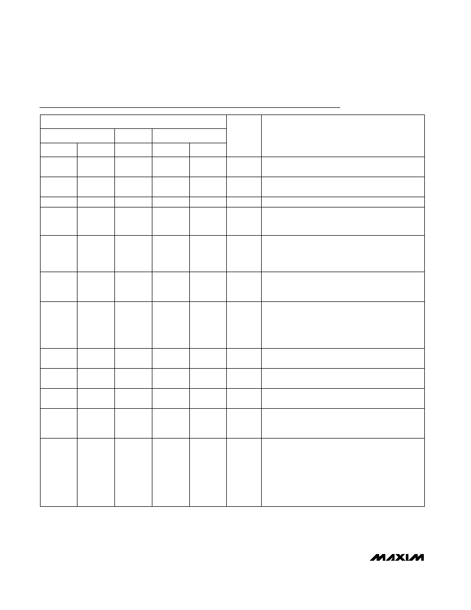
Pin Description
2
Parallel Data Bit D0 when SER/PAR = GND. Serial
input when SER/PAR = VCC.
3, 5
Output Buffer Address Lines
4, 6, 8, 10
4, 6, 8, 10,
12, 14, 16,
18
Video Input Lines
7
Asynchronous Control Line. When LOAD = VCC, all the
400
internal active loads are on. When LOAD = GND,
external 400
loads must be used. The buffers must
have a resistive load to maintain stability.
9
Digital Ground. DGND pins must have the same
potential and be bypassed to AGND. DGND should
be within ±0.3V of AGND.
11
When this control line is high, the 2nd-rank registers
are loaded with the rising edge of LATCH. If this con-
trol line is low, the 2nd-rank registers are transparent
when LATCH is low, passing data directly from the
1st-rank registers to the decoders.
—
12–16, 18,
22–26
No connection. Not internally connected.
12
17
Connect to VCC for serial mode; connect to GND for
parallel mode.
13
19, 30
Negative Supply. All V- pins must be connected to each
other and bypassed to GND separately (Figure 2).
14
20
In serial mode, WR (write) shifts data into the input regis-
ter. In parallel mode, WR loads data into the 1st-rank
registers. Data is latched on the rising edge.
1
2
1
Parallel Data Bit D1 when SER/PAR = GND. Serial out-
put for cascading multiple parts when SER/PAR = VCC.
D1/
SER OUT
2
3
3, 4, 6
4, 5, 7
5, 7, 9, 11,
13, 15, 17,
19
6, 8, 10, 13,
15, 17, 19,
21
8
9
10, 12
11, 14
14
16
—
1, 12, 23,
34
18
20
20, 34
22, 38
21
24
D0/SER IN
A_
IN_
LOAD
DGND
EDGE/
LEVEL
N.C.
SER/PAR
V-
WR
MAX4360
MAX4456
MAX4359
DIP
PLCC
SO
SSOP
FUNCTION
NAME
PIN
15
21
If EDGE/LEVEL = VCC, data is loaded from the 1st-
rank registers to the 2nd-rank registers on the rising
edge of LATCH. If EDGE/LEVEL = GND, data is
loaded while LATCH = GND. In addition, data is
loaded during the execution of parallel-mode func-
tions 1011 through 1110, or if LATCH = VCC during
the execution of the parallel-mode “software-latch”
command (1111).
22
25
LATCH
相关PDF资料 |
PDF描述 |
|---|---|
| MAX4358ECE+T | IC VIDEO CROSSPOINT SWIT 144TQFP |
| MAX4358ECE+D | IC VIDEO CROSSPOINT SWIT 144TQFP |
| DS72613RB120FPV | IC SUPERH MPU ROMLESS 176LQFP |
| MAX4358ECE+ | IC VIDEO CROSSPOINT SWIT 144TQFP |
| DG423DY+ | IC SWITCH DUAL SPDT 16SOIC |
相关代理商/技术参数 |
参数描述 |
|---|---|
| MAX445CPG | 制造商:Maxim Integrated Products 功能描述: |
| MAX4460ESA | 功能描述:仪表放大器 RoHS:否 制造商:Texas Instruments 通道数量: 输入补偿电压:150 V 可用增益调整: 最大输入电阻:10 kOhms 共模抑制比(最小值):88 dB 工作电源电压:2.7 V to 36 V 电源电流:200 uA 最大工作温度:+ 125 C 最小工作温度:- 40 C 封装 / 箱体:MSOP-8 封装:Bulk |
| MAX4460ESA+ | 功能描述:仪表放大器 3V/5V Single-Supply Rail-Rail RoHS:否 制造商:Texas Instruments 通道数量: 输入补偿电压:150 V 可用增益调整: 最大输入电阻:10 kOhms 共模抑制比(最小值):88 dB 工作电源电压:2.7 V to 36 V 电源电流:200 uA 最大工作温度:+ 125 C 最小工作温度:- 40 C 封装 / 箱体:MSOP-8 封装:Bulk |
| MAX4460ESA+T | 功能描述:仪表放大器 3V/5V Single-Supply Rail-Rail RoHS:否 制造商:Texas Instruments 通道数量: 输入补偿电压:150 V 可用增益调整: 最大输入电阻:10 kOhms 共模抑制比(最小值):88 dB 工作电源电压:2.7 V to 36 V 电源电流:200 uA 最大工作温度:+ 125 C 最小工作温度:- 40 C 封装 / 箱体:MSOP-8 封装:Bulk |
| MAX4460ESA-T | 功能描述:仪表放大器 RoHS:否 制造商:Texas Instruments 通道数量: 输入补偿电压:150 V 可用增益调整: 最大输入电阻:10 kOhms 共模抑制比(最小值):88 dB 工作电源电压:2.7 V to 36 V 电源电流:200 uA 最大工作温度:+ 125 C 最小工作温度:- 40 C 封装 / 箱体:MSOP-8 封装:Bulk |
发布紧急采购,3分钟左右您将得到回复。