- 您现在的位置:买卖IC网 > PDF目录11050 > MAX4501EPA (Maxim Integrated Products)IC SWITCH SPST 8DIP PDF资料下载
参数资料
| 型号: | MAX4501EPA |
| 厂商: | Maxim Integrated Products |
| 文件页数: | 6/8页 |
| 文件大小: | 0K |
| 描述: | IC SWITCH SPST 8DIP |
| 产品培训模块: | Lead (SnPb) Finish for COTS Obsolescence Mitigation Program |
| 标准包装: | 50 |
| 功能: | 开关 |
| 电路: | 1 x SPST- NO |
| 导通状态电阻: | 250 欧姆 |
| 电压电源: | 单电源 |
| 电压 - 电源,单路/双路(±): | 2 V ~ 12 V |
| 电流 - 电源: | 1µA |
| 工作温度: | -40°C ~ 85°C |
| 安装类型: | 通孔 |
| 封装/外壳: | 8-DIP(0.300",7.62mm) |
| 供应商设备封装: | 8-PDIP |
| 包装: | 管件 |
MAX4501/MAX4502
Low-Voltage, SPST, CMOS Analog Switches
6
_______________________________________________________________________________________
Applications Information
Power-Supply Considerations
The MAX4501/MAX4502 are constructed like most
CMOS analog switches, except they have only two sup-
ply pins: V+ and GND. V+ and GND drive the internal
CMOS switches and set the analog voltage limits of the
switch. Reverse ESD-protection diodes are internally
connected between each analog signal pin and both
V+ and GND. One of these diodes conducts if any ana-
log signal exceeds V+ or GND. During normal opera-
tion, these and other reverse-biased ESD diodes leak,
forming the only current drawn from V+ or GND.
Virtually all the analog leakage current comes from the
ESD diodes. Although the ESD diodes on a given sig-
nal pin are identical and therefore fairly well balanced,
they are reverse biased differently. Each is biased by
either V+ or GND and the analog signal. This means
their leakages will vary as the signal varies. The differ-
ence in the two diode leakages to the V+ and GND
pins constitutes the analog signal-path leakage current.
All analog leakage current flows between each pin and
one of the supply terminals, not to the other switch ter-
minal. This is why both sides of a given switch can
show leakage currents of the same or opposite polarity.
There is no connection between the analog-signal
paths and V+ or GND.
V+ and GND also power the internal logic and logic-
level translators, and set the input logic limits. The
logic-level translators convert the logic levels to
switched V+ and GND signals to drive the analog sig-
nal gates. This drive signal is the only connection
between the logic supplies (and signals) and the ana-
log supplies. COM, NO, and NC pins have ESD-protec-
tion diodes to V+ and GND.
The logic-level thresholds are CMOS/TTL compatible
when V+ is +5V. As V+ rises, the threshold increases
slightly. When V+ reaches +12V, the logic-level thresh-
old is about 3V—above the TTL guaranteed high-level
minimum of 2.8V, but still compatible with CMOS out-
puts.
Do not connect the MAX4501/MAX4502’s V+ pin to
+3V and then connect the logic-level pins to TTL
logic-level signals. TTL levels can exceed +3V and
violate the absolute maximum ratings, damaging
the part and/or external circuits.
High-Frequency Performance
In 50
systems, signal response is reasonably flat up
to 250MHz (see Typical Operating Characteristics).
Above 20MHz, the on-response has several minor
peaks that are highly layout dependent. The problem is
not in turning the switch on; it’s in turning it off. The off-
state switch acts like a capacitor and passes higher
frequencies with less attenuation. At 10MHz, off-isola-
tion is about -60dB in 50
systems, decreasing
approximately 20dB per decade as frequency increas-
es. Higher circuit impedances also cause off-isolation
to decrease. Adjacent channel attenuation is about 3dB
above that of a bare IC socket, and is due entirely to
capacitive coupling.
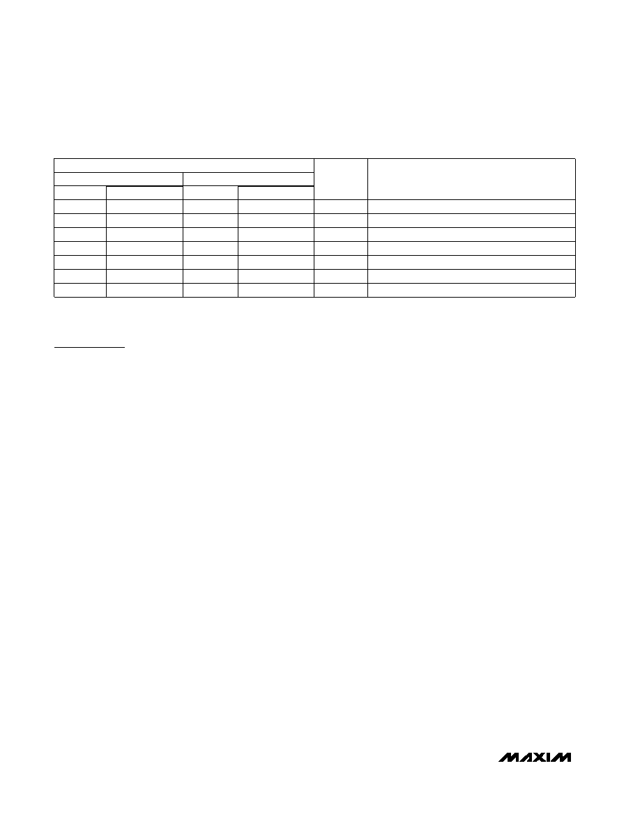
______________________________________________________________Pin Description
Note: NO, NC, and COM pins are identical and interchangeable. Any may be considered as an input or an output; signals pass
equally well in both directions.
FUNCTION
NAME
MAX4501
MAX4502
SO/DIP
SC70-5/SOT23-5
SO/DIP
SC70-5/SOT23-5
Positive Supply-Voltage Input (analog and digital)
PIN
1
COM
Analog Switch Common Terminal
2, 3, 5
—
2, 3, 5
—
N.C.
No Connection. Not internally connected.
4
5
V+
6
4
6
4
IN
Digital Control Input
7
3
7
3
GND
Ground
8
2
—
NO
Analog Switch (normally open)
—
8
2
NC
Analog Switch (normally closed)
5
4
相关PDF资料 |
PDF描述 |
|---|---|
| MAX4501CSA | IC SWITCH SPST 8SOIC |
| MAX4066AEPD | IC SWITCH QUAD SPST 14DIP |
| MAX4053ESE | IC MULTIPLEXER TRPL 2X1 16SOIC |
| MAX4053EPE | IC MULTIPLEXER TRPL 2X1 16DIP |
| MAX4053CSE | IC MULTIPLEXER TRPL 2X1 16SOIC |
相关代理商/技术参数 |
参数描述 |
|---|---|
| MAX4501ESA | 功能描述:模拟开关 IC RoHS:否 制造商:Texas Instruments 开关数量:2 开关配置:SPDT 开启电阻(最大值):0.1 Ohms 切换电压(最大): 开启时间(最大值): 关闭时间(最大值): 工作电源电压:2.7 V to 4.5 V 最大工作温度:+ 85 C 安装风格:SMD/SMT 封装 / 箱体:DSBGA-16 |
| MAX4501ESA+ | 功能描述:模拟开关 IC Low-Voltage SPST CMOS Analog Switch RoHS:否 制造商:Texas Instruments 开关数量:2 开关配置:SPDT 开启电阻(最大值):0.1 Ohms 切换电压(最大): 开启时间(最大值): 关闭时间(最大值): 工作电源电压:2.7 V to 4.5 V 最大工作温度:+ 85 C 安装风格:SMD/SMT 封装 / 箱体:DSBGA-16 |
| MAX4501ESA+T | 功能描述:模拟开关 IC Low-Voltage SPST CMOS Analog Switch RoHS:否 制造商:Texas Instruments 开关数量:2 开关配置:SPDT 开启电阻(最大值):0.1 Ohms 切换电压(最大): 开启时间(最大值): 关闭时间(最大值): 工作电源电压:2.7 V to 4.5 V 最大工作温度:+ 85 C 安装风格:SMD/SMT 封装 / 箱体:DSBGA-16 |
| MAX4501ESA-T | 功能描述:模拟开关 IC RoHS:否 制造商:Texas Instruments 开关数量:2 开关配置:SPDT 开启电阻(最大值):0.1 Ohms 切换电压(最大): 开启时间(最大值): 关闭时间(最大值): 工作电源电压:2.7 V to 4.5 V 最大工作温度:+ 85 C 安装风格:SMD/SMT 封装 / 箱体:DSBGA-16 |
| MAX4501EUK | 制造商:Maxim Integrated Products 功能描述:NORMALLY OPEN LOW-VOLTAGE,SPST,CMOS ANALOG SWITCH - Cut Tape Product |
发布紧急采购,3分钟左右您将得到回复。