- 您现在的位置:买卖IC网 > PDF目录4592 > MAX4507CPN+ (Maxim Integrated Products)IC SIGNAL LINE PROTECTOR 18-DIP PDF资料下载
参数资料
| 型号: | MAX4507CPN+ |
| 厂商: | Maxim Integrated Products |
| 文件页数: | 11/12页 |
| 文件大小: | 0K |
| 描述: | IC SIGNAL LINE PROTECTOR 18-DIP |
| 产品培训模块: | Lead (SnPb) Finish for COTS Obsolescence Mitigation Program |
| 标准包装: | 20 |
| 类型: | 过压防护 |
| 应用: | 控制系统 |
| 安装类型: | 通孔 |
| 封装/外壳: | 18-DIP(0.300",7.62mm) |
| 供应商设备封装: | 18-PDIP |
| 包装: | 管件 |
MAX4506/MAX4507
Fault-Protected, High-Voltage
Signal-Line Protectors
8
_______________________________________________________________________________________
Two clamp circuits limit the output voltage to within the
supply voltages. When the power supplies are off, any
input voltage applied at IN turns off both N1 and P1,
and OUT is clamped to 0V.
Normal Operation
When power is applied, each protector acts as a resis-
tor in series with the signal path. Any voltage source on
the “input” side of the switch will be conducted through
the protector to the output (Figure 2).
When the output load is resistive, it draws current
through the protector. The internal resistance is typically
less than 100
. High-impedance loads are relatively
unaffected by the presence of the MAX4506/MAX4507.
The protector’s path resistance is a function of the supply
voltage and the signal voltage (see Typical Operating
Characteristics).
Fault Protection, Power Off
When power is off (i.e., V+ = V- = 0), the protector is a
virtual open circuit. With up to ±40V applied to the input
pin, the output pin will be 0V.
Fault Protection, Power On
A fault condition exists when the voltage on the IN_
exceeds either supply rail. This definition is valid when
power is on or off, as well as during all states while
power ramps up or down.
Applications Information
Supplying Power Through External ICs
The MAX4506/MAX4507 have low supply currents
(<250A), which allows the supply pins to be driven by
other active circuitry instead of connected directly to
the power sources. In this configuration, the parts can
be used as driven fault-protected switches with V+ or
V- used as the control pins. For example, with the V-
pin grounded, the output of a CMOS gate can drive the
V+ pin to turn the device on and off. This can effectively
connect and disconnect three (MAX4506) or eight
(MAX4507) separate signal lines at once. Ensure that
the driving source(s) does not drive the V+ pin more
negative than the V- pin.
Figure 3 shows a simple turn-on delay that takes
advantage of the MAX4506’s low power consumption.
The two RC networks cause gradual application of
power to the MAX4506, which in turn applies the input
signals smoothly after the amplifier has stabilized. The
two diodes discharge the two capacitors rapidly when
the power turns off. Note that the IC used to supply
power to the MAX4506/MAX4507 must be able to sup-
ply enough current to maintain the load voltage at the
supply rail in a fault condition.
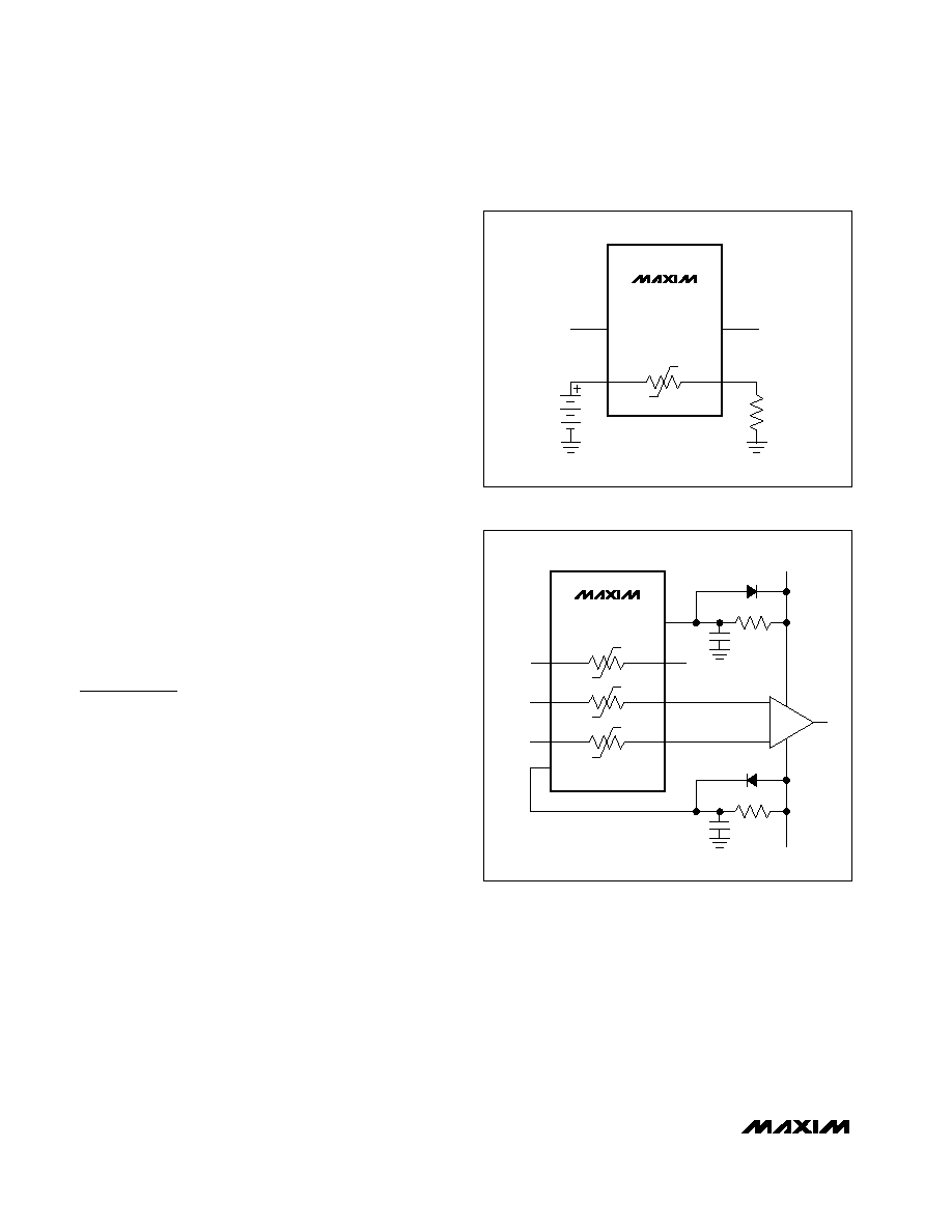
MAX4506
ROUT
VIN
IN1
V-
V+
1
4
7
8
OUT1
Figure 2. Application Circuit
MAX4506
IN3
V-
-15V
V+
+15V
3
4
5
10
F
10
F
OUT3
IN2
26
OUT2
IN1
17
OUT1
8
100k
100k
OP AMP
Figure 3. Turn-On Delay
相关PDF资料 |
PDF描述 |
|---|---|
| DS1402-BR8+ | CABLE 8' BUTTON TO RJ11 |
| LFXP6E-3F256C | IC FPGA 5.8KLUTS 188I/O 256-BGA |
| DS1402-RP3+ | CABLE TOUCH & HOLD PROBE |
| LFXP6C-3F256C | IC FPGA 5.8KLUTS 188I/O 256-BGA |
| DS9100-A+ | CONTACT TOUCH AND HOLD |
相关代理商/技术参数 |
参数描述 |
|---|---|
| MAX4507CPN+ | 功能描述:模拟开关 IC Fault-Protected Signal-Line Protectr RoHS:否 制造商:Texas Instruments 开关数量:2 开关配置:SPDT 开启电阻(最大值):0.1 Ohms 切换电压(最大): 开启时间(最大值): 关闭时间(最大值): 工作电源电压:2.7 V to 4.5 V 最大工作温度:+ 85 C 安装风格:SMD/SMT 封装 / 箱体:DSBGA-16 |
| MAX4507CWN | 功能描述:模拟开关 IC RoHS:否 制造商:Texas Instruments 开关数量:2 开关配置:SPDT 开启电阻(最大值):0.1 Ohms 切换电压(最大): 开启时间(最大值): 关闭时间(最大值): 工作电源电压:2.7 V to 4.5 V 最大工作温度:+ 85 C 安装风格:SMD/SMT 封装 / 箱体:DSBGA-16 |
| MAX4507CWN+ | 功能描述:模拟开关 IC Fault-Protected Signal-Line Protectr RoHS:否 制造商:Texas Instruments 开关数量:2 开关配置:SPDT 开启电阻(最大值):0.1 Ohms 切换电压(最大): 开启时间(最大值): 关闭时间(最大值): 工作电源电压:2.7 V to 4.5 V 最大工作温度:+ 85 C 安装风格:SMD/SMT 封装 / 箱体:DSBGA-16 |
| MAX4507CWN+T | 功能描述:模拟开关 IC Fault-Protected Signal-Line Protectr RoHS:否 制造商:Texas Instruments 开关数量:2 开关配置:SPDT 开启电阻(最大值):0.1 Ohms 切换电压(最大): 开启时间(最大值): 关闭时间(最大值): 工作电源电压:2.7 V to 4.5 V 最大工作温度:+ 85 C 安装风格:SMD/SMT 封装 / 箱体:DSBGA-16 |
| MAX4507CWN-T | 功能描述:模拟开关 IC RoHS:否 制造商:Texas Instruments 开关数量:2 开关配置:SPDT 开启电阻(最大值):0.1 Ohms 切换电压(最大): 开启时间(最大值): 关闭时间(最大值): 工作电源电压:2.7 V to 4.5 V 最大工作温度:+ 85 C 安装风格:SMD/SMT 封装 / 箱体:DSBGA-16 |
发布紧急采购,3分钟左右您将得到回复。