- 您现在的位置:买卖IC网 > PDF目录11120 > MAX4508ESE+T (Maxim Integrated Products)IC MULTIPLEXER 8X1 16SOIC PDF资料下载
参数资料
| 型号: | MAX4508ESE+T |
| 厂商: | Maxim Integrated Products |
| 文件页数: | 2/18页 |
| 文件大小: | 0K |
| 描述: | IC MULTIPLEXER 8X1 16SOIC |
| 产品培训模块: | Lead (SnPb) Finish for COTS Obsolescence Mitigation Program |
| 标准包装: | 2,500 |
| 功能: | 多路复用器 |
| 电路: | 1 x 8:1 |
| 导通状态电阻: | 400 欧姆 |
| 电压电源: | 单/双电源 |
| 电压 - 电源,单路/双路(±): | 9 V ~ 36 V,±4.5 V ~ 20 V |
| 电流 - 电源: | 1µA |
| 工作温度: | -40°C ~ 85°C |
| 安装类型: | 表面贴装 |
| 封装/外壳: | 16-SOIC(0.154",3.90mm 宽) |
| 供应商设备封装: | 16-SOIC |
| 包装: | 带卷 (TR) |
MAX4508/MAX4509
When the NO_ voltage goes beyond supply rails (fault
condition), the NO_ input becomes high impedance
regardless of the switch state or load resistance. When
power is removed, and the fault protection is still in
effect, the NO_ terminals are a virtual open circuit. The
fault can be up to ±40V, with V+ = V- = 0. If the switch
is on, the COM_ output current is furnished from the V+
or V- pin by “booster” FETs connected to each supply
pin. These FETs can source or sink up to 10mA.
The COM_ pins are not fault protected. If a voltage
source is connected to any COM_ pin, it should be lim-
ited to the supply voltages. Exceeding the supply volt-
age will cause high currents to flow through the ESD
protection diodes, damaging the device (see Absolute
Maximum Ratings).
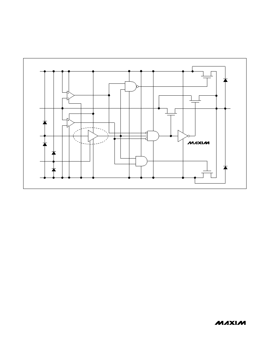
Figure 1 shows the internal construction, with the ana-
log signal paths shown in bold. A single normally open
(NO) switch is shown. The analog switch is formed by
the parallel combination of N-channel FET N1 and P-
channel FET P1, which are driven on and off simultane-
ously, according to the input fault condition and the
logic level state.
NO_ Input Voltage
The maximum allowable input voltage for safe opera-
tion depends on whether supplies are on or off and the
load configuration at the COM output. If COM is re-
ferred to a voltage other than ground, but within the
supplies, VNO_ may range higher or lower than the sup-
plies provided the absolute value of
VNO_ - VCOM_ is
less than 40V. For example, if the load is referred to
+10V at COM_, then the NO_ voltage range can be
from +50V to -30V. As another example, if the load is
connected to -10V at COM_, the NO_ voltage range is
limited to -50V to +30V.
If the supplies are ±15V and COM is referenced to
ground through a load, the maximum NO_ voltage is
±25V. If the supplies are off and the COM output is ref-
erenced to ground, the maximum NO_ voltage is ±40V.
Normal Operation
Two comparators continuously compare the voltage on
the NO_ pin with V+ and V- supply voltages. When the
signal on NO_ is between V+ and V-, the multiplexer
behaves normally, with FETs N1 and P1 turning on and
off in response to A_ signals (Figure 1). The parallel
Fault-Protected, High-Voltage Single 8-to-1/
Dual 4-to-1 Multiplexers with Output Clamps
10
______________________________________________________________________________________
NORMALLY OPEN SWITCH CONSTRUCTION
COM_
P2
P1
N1
ON
LOW
FAULT
HIGH
FAULT
V+
NO_
A-
GWD
ESO CODE
V-
N2
MAX4508
MAX4509
Figure 1. Functional Diagram
相关PDF资料 |
PDF描述 |
|---|---|
| VE-BWH-IY-F3 | CONVERTER MOD DC/DC 52V 50W |
| MAX4509ESE+T | IC MULTIPLEXER DUAL 4X1 16SOIC |
| VE-BWH-IY-F1 | CONVERTER MOD DC/DC 52V 50W |
| MAX4708ESE+T | IC MULTIPLEXER 8X1 16SOIC |
| VE-BWF-IY-F4 | CONVERTER MOD DC/DC 72V 50W |
相关代理商/技术参数 |
参数描述 |
|---|---|
| MAX4508ESE-W | 制造商:Maxim Integrated Products 功能描述:16 PINS N.SO PKG - Bulk |
| MAX4508MJE | 功能描述:多路器开关 IC HV MULTIPLEXER RoHS:否 制造商:Texas Instruments 通道数量:1 开关数量:4 开启电阻(最大值):7 Ohms 开启时间(最大值): 关闭时间(最大值): 传播延迟时间:0.25 ns 工作电源电压:2.3 V to 3.6 V 工作电源电流: 最大工作温度:+ 85 C 安装风格:SMD/SMT 封装 / 箱体:UQFN-16 |
| MAX4509C/D | 功能描述:多路器开关 IC RoHS:否 制造商:Texas Instruments 通道数量:1 开关数量:4 开启电阻(最大值):7 Ohms 开启时间(最大值): 关闭时间(最大值): 传播延迟时间:0.25 ns 工作电源电压:2.3 V to 3.6 V 工作电源电流: 最大工作温度:+ 85 C 安装风格:SMD/SMT 封装 / 箱体:UQFN-16 |
| MAX4509CPE | 功能描述:多路器开关 IC RoHS:否 制造商:Texas Instruments 通道数量:1 开关数量:4 开启电阻(最大值):7 Ohms 开启时间(最大值): 关闭时间(最大值): 传播延迟时间:0.25 ns 工作电源电压:2.3 V to 3.6 V 工作电源电流: 最大工作温度:+ 85 C 安装风格:SMD/SMT 封装 / 箱体:UQFN-16 |
| MAX4509CPE+ | 功能描述:多路器开关 IC 4:1 2Ch Fault Prtctd Analog MUX RoHS:否 制造商:Texas Instruments 通道数量:1 开关数量:4 开启电阻(最大值):7 Ohms 开启时间(最大值): 关闭时间(最大值): 传播延迟时间:0.25 ns 工作电源电压:2.3 V to 3.6 V 工作电源电流: 最大工作温度:+ 85 C 安装风格:SMD/SMT 封装 / 箱体:UQFN-16 |
发布紧急采购,3分钟左右您将得到回复。