- 您现在的位置:买卖IC网 > PDF目录11165 > MAX4516EUK-T (Maxim Integrated Products)IC SWITCH SPST SOT23-5 PDF资料下载
参数资料
| 型号: | MAX4516EUK-T |
| 厂商: | Maxim Integrated Products |
| 文件页数: | 5/8页 |
| 文件大小: | 0K |
| 描述: | IC SWITCH SPST SOT23-5 |
| 产品培训模块: | Lead (SnPb) Finish for COTS Obsolescence Mitigation Program |
| 标准包装: | 2,500 |
| 功能: | 开关 |
| 电路: | 1 x SPST- NO |
| 导通状态电阻: | 20 欧姆 |
| 电压电源: | 双电源 |
| 电压 - 电源,单路/双路(±): | ±1 V ~ 6 V |
| 电流 - 电源: | -30µA,40µA |
| 工作温度: | -40°C ~ 85°C |
| 安装类型: | 表面贴装 |
| 封装/外壳: | SC-74A,SOT-753 |
| 供应商设备封装: | SOT-23-5 |
| 包装: | 带卷 (TR) |
MAX4517
__________Applications Information
Power-Supply Considerations
The MAX4516/MAX4517 operate with power-supply
voltages from ±1V to ±6V, but are tested and guaran-
teed only with ±5V supplies. Similarly, they will operate
with a single +2V to +12V supply, but logic-level inputs
can shift with higher voltages. The pin-compatible
MAX4514/MAX4515 are recommended for use with a
single supply.
The MAX4516/MAX4517 construction is typical of most
CMOS analog switches, except that they have only two
supply pins: V+ and V-. V+ and V- drive the internal
CMOS switches and set their analog voltage limits.
Reverse ESD-protection diodes are internally connected
between each analog-signal pin and both V+ and V-.
One of these diodes conducts if any analog signal
exceeds V+ or V-.
Virtually all the analog leakage current comes from the
ESD diodes to V+ or V-. Although the ESD diodes on a
given signal pin are identical and therefore fairly well
balanced, they are reverse biased differently. Each is
biased by either V+ or V- and the analog signal. This
means their leakages will vary as the signal varies. The
difference in the two diode leakages to the V+ and V-
pins constitutes the analog-signal-path leakage current.
All analog leakage current flows between each pin and
one of the supply terminals, not to the other switch ter-
minal. This is why both sides of a given switch can
show leakage currents of the same or opposite polarity.
There is no connection between the analog-signal
paths and V+ or V-.
V+ and V- also power the internal logic and logic-level
translators. The logic-level translators convert the logic
levels to switched V+ and V- signals to drive the analog
signal gates.
Logic-Level Thresholds
The logic-level thresholds are CMOS-compatible but
not TTL-compatible. Since these parts have no
ground pin, the logic-level threshold is referenced to
V+. The threshold limits are V+ = -1.5V and V+ = -3.5V
for V+ levels between +6V and +3V. When V+ = +2V,
the logic threshold is approximately 0.6V.
Do not connect the MAX4516/MAX4517’s V+ to +3V
and then connect the logic-level pins to logic-level
signals that operate from a +5V supply. TTL levels
can exceed +3V and violate the absolute maximum
ratings, damaging the part and/or external circuits.
High-Frequency Performance
In 50
systems, signal response is reasonably flat up
to 250MHz (see
Typical Operating Characteristics).
Above 20MHz, the on response has several minor
peaks that are highly layout dependent. The problem is
not in turning the switch on; it’s in turning it off. The off-
state switch acts like a capacitor and passes higher fre-
quencies with less attenuation. At 10MHz, off isolation is
about -48dB in 50
systems, decreasing (approximate-
ly 20dB per decade) as frequency increases. Higher cir-
cuit impedances also cause off isolation to decrease.
Off isolation is about 3dB above that of a bare IC sock-
et, and is due entirely to capacitive coupling.
MAX4516/MAX4517
Dual-Supply, Low-On-Resistance,
SPST, CMOS Analog Switches
_______________________________________________________________________________________
5
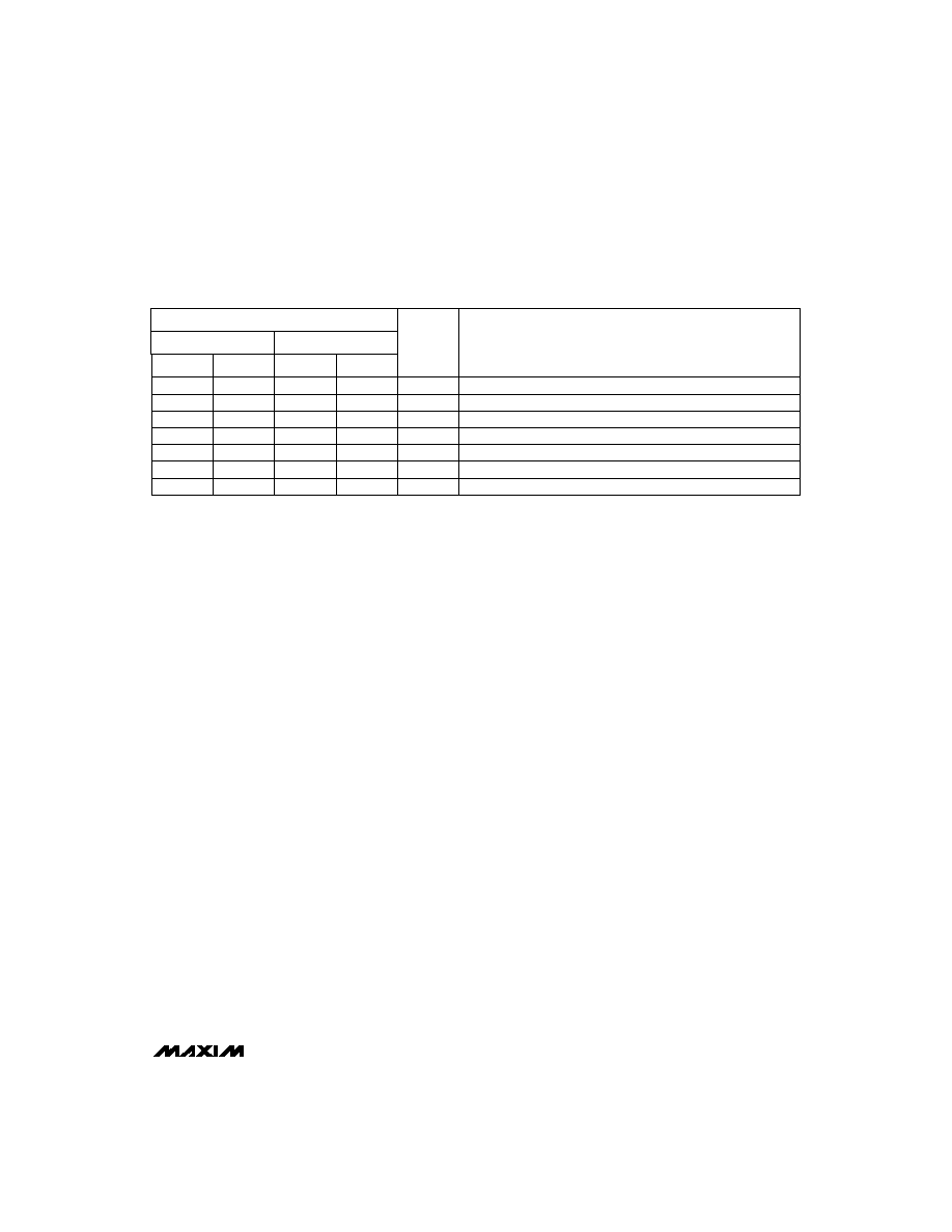
______________________________________________________________Pin Description
SOT23-5
DIP/SO
SOT23-5
DIP/SO
Analog Switch (normally closed)
—
3
2
4
5
—
Negative Supply-Voltage Input (analog and digital)
1
7
Analog Switch (normally open)
8
2
8
3
Digital Control Input
—
6
Positive Supply-Voltage Input (analog and digital)
4
No Connect (not internally connected)
5
2, 3, 5
Analog Switch Common Terminal
1
—
1
7
—
6
4
2, 3, 5
1
NC
V-
NO
IN
V+
N.C.
COM
Note: NO, NC, and COM pins are identical and interchangeable. Any may be considered as an input or an output; signals pass
equally well in both directions.
NAME
FUNCTION
MAX4516
MAX4517
PIN
相关PDF资料 |
PDF描述 |
|---|---|
| MAX4594ELT+T | IC SWITCH SPST 6UDFN |
| MAX4595EXK+T | IC SWITCH SPST SC70-5 |
| MAX4596EXK+T | IC SWITCH SPST SC70-5 |
| MAX4517EUK+T | IC SWITCH SPST SOT23-5 |
| VI-B4J-CU-B1 | CONVERTER MOD DC/DC 36V 200W |
相关代理商/技术参数 |
参数描述 |
|---|---|
| MAX4516MJA | 功能描述:模拟开关 IC RoHS:否 制造商:Texas Instruments 开关数量:2 开关配置:SPDT 开启电阻(最大值):0.1 Ohms 切换电压(最大): 开启时间(最大值): 关闭时间(最大值): 工作电源电压:2.7 V to 4.5 V 最大工作温度:+ 85 C 安装风格:SMD/SMT 封装 / 箱体:DSBGA-16 |
| MAX4517C/D | 功能描述:模拟开关 IC RoHS:否 制造商:Texas Instruments 开关数量:2 开关配置:SPDT 开启电阻(最大值):0.1 Ohms 切换电压(最大): 开启时间(最大值): 关闭时间(最大值): 工作电源电压:2.7 V to 4.5 V 最大工作温度:+ 85 C 安装风格:SMD/SMT 封装 / 箱体:DSBGA-16 |
| MAX4517CPA | 功能描述:模拟开关 IC RoHS:否 制造商:Texas Instruments 开关数量:2 开关配置:SPDT 开启电阻(最大值):0.1 Ohms 切换电压(最大): 开启时间(最大值): 关闭时间(最大值): 工作电源电压:2.7 V to 4.5 V 最大工作温度:+ 85 C 安装风格:SMD/SMT 封装 / 箱体:DSBGA-16 |
| MAX4517CSA | 功能描述:模拟开关 IC RoHS:否 制造商:Texas Instruments 开关数量:2 开关配置:SPDT 开启电阻(最大值):0.1 Ohms 切换电压(最大): 开启时间(最大值): 关闭时间(最大值): 工作电源电压:2.7 V to 4.5 V 最大工作温度:+ 85 C 安装风格:SMD/SMT 封装 / 箱体:DSBGA-16 |
| MAX4517CSA-T | 功能描述:模拟开关 IC RoHS:否 制造商:Texas Instruments 开关数量:2 开关配置:SPDT 开启电阻(最大值):0.1 Ohms 切换电压(最大): 开启时间(最大值): 关闭时间(最大值): 工作电源电压:2.7 V to 4.5 V 最大工作温度:+ 85 C 安装风格:SMD/SMT 封装 / 箱体:DSBGA-16 |
发布紧急采购,3分钟左右您将得到回复。