- 您现在的位置:买卖IC网 > PDF目录11048 > MAX4525CUB (Maxim Integrated Products)IC MULTIPLEXER 2X2 10UMAX PDF资料下载
参数资料
| 型号: | MAX4525CUB |
| 厂商: | Maxim Integrated Products |
| 文件页数: | 13/14页 |
| 文件大小: | 0K |
| 描述: | IC MULTIPLEXER 2X2 10UMAX |
| 产品培训模块: | Lead (SnPb) Finish for COTS Obsolescence Mitigation Program |
| 标准包装: | 50 |
| 功能: | 多路复用器 |
| 电路: | 1 x 2:2 |
| 导通状态电阻: | 150 欧姆 |
| 电压电源: | 单电源 |
| 电压 - 电源,单路/双路(±): | 2 V ~ 12 V |
| 电流 - 电源: | 1µA |
| 工作温度: | 0°C ~ 70°C |
| 安装类型: | 表面贴装 |
| 封装/外壳: | 10-TFSOP,10-MSOP(0.118",3.00mm 宽) |
| 供应商设备封装: | 10-µMAX |
| 包装: | 管件 |
MAX4524/MAX4525
There is no connection between the analog signal
paths and GND. V+ and GND power the internal logic
and logic-level translators, and set both the input and
output logic limits. The logic-level translators convert
the logic levels into switched V+ and GND signals to
drive the gates of the analog signals. This drive signal
is the only connection between the logic supplies (and
signals) and the analog supplies. V+ has an ESD-pro-
tection diode to GND.
Low-Voltage Operation
These devices operate from a single supply between
+2V and +12V. At room temperature, they actually
“work” with a single supply at near or below +1.7V,
although as supply voltage decreases, switch on-resis-
tance and switching times become very high.
High-Frequency Performance
In 50
systems, signal response is reasonably flat up
to 50MHz (see Typical Operating Characteristics).
Above 20MHz, the on-response has several minor
peaks, which are highly layout dependent. The problem
is not turning the switch on, but turning it off. The off-
state switch acts like a capacitor, and passes higher
frequencies with less attenuation. At 10MHz, off-isola-
tion is about -50dB in 50
systems, becoming worse
(approximately 20dB per decade) as frequency
increases. Higher circuit impedances also degrade off-
isolation. Adjacent channel attenuation is about 3dB
above that of a bare IC socket, and is entirely due to
capacitive coupling.
Low-Voltage, Single-Supply
Multiplexer and Switch
8
_______________________________________________________________________________________
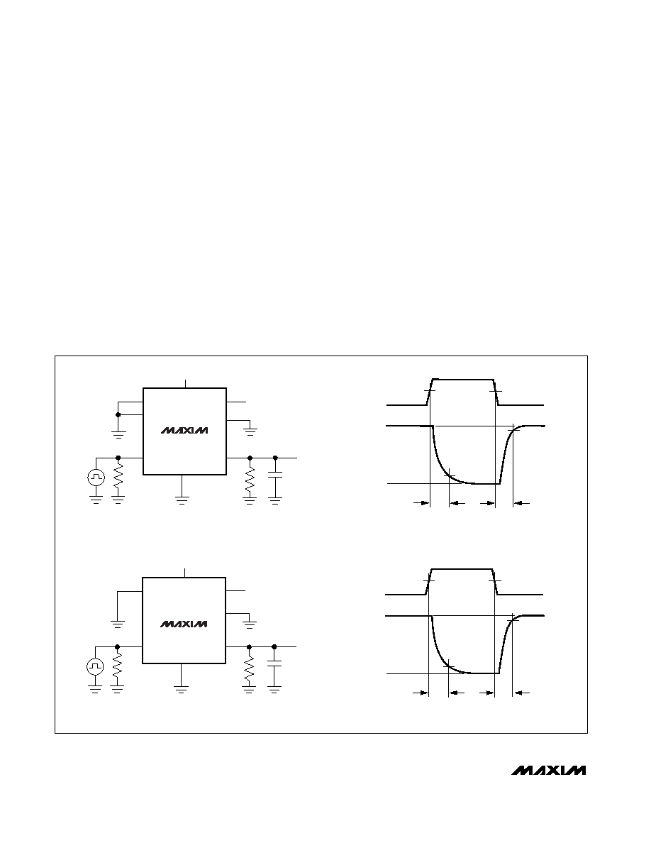
_________________________________Test Circuits/Timing Diagrams (continued)
50%
tOFF
V+
0V
VNO0
VOUT
VINH
0V
90%
tON
50%
tOFF
V+
0V
VNO_
VOUT
VINH
0V
90%
tON
VINH
V+
VOUT
GND
V+
ADDB
ADDA
INH
NO0
NO1–NO3
COM
V+
MAX4524
300
50
35pF
V+
VOUT
GND
V+
ADD
INH
NO_
NC_
COM_
V+
MAX4525
300
35pF
50
REPEAT TEST FOR EACH SECTION.
Figure 2. Inhibit Switching Times
相关PDF资料 |
PDF描述 |
|---|---|
| MAX4524CUB | IC MULTIPLEXER 4X1 10UMAX |
| MAX4523CEE | IC SWITCH QUAD SPST 16QSOP |
| MAX4522ESE | IC SWITCH QUAD SPST 16SOIC |
| VE-BTZ-IW-F3 | CONVERTER MOD DC/DC 2V 40W |
| MAX4521CSE | IC SWITCH QUAD SPST 16SOIC |
相关代理商/技术参数 |
参数描述 |
|---|---|
| MAX4525CUB+ | 功能描述:模拟开关 IC DPDT 1Ch/SPDT 2Ch Analog Switch RoHS:否 制造商:Texas Instruments 开关数量:2 开关配置:SPDT 开启电阻(最大值):0.1 Ohms 切换电压(最大): 开启时间(最大值): 关闭时间(最大值): 工作电源电压:2.7 V to 4.5 V 最大工作温度:+ 85 C 安装风格:SMD/SMT 封装 / 箱体:DSBGA-16 |
| MAX4525CUB+T | 功能描述:模拟开关 IC DPDT 1Ch/SPDT 2Ch Analog Switch RoHS:否 制造商:Texas Instruments 开关数量:2 开关配置:SPDT 开启电阻(最大值):0.1 Ohms 切换电压(最大): 开启时间(最大值): 关闭时间(最大值): 工作电源电压:2.7 V to 4.5 V 最大工作温度:+ 85 C 安装风格:SMD/SMT 封装 / 箱体:DSBGA-16 |
| MAX4525CUB-T | 功能描述:模拟开关 IC RoHS:否 制造商:Texas Instruments 开关数量:2 开关配置:SPDT 开启电阻(最大值):0.1 Ohms 切换电压(最大): 开启时间(最大值): 关闭时间(最大值): 工作电源电压:2.7 V to 4.5 V 最大工作温度:+ 85 C 安装风格:SMD/SMT 封装 / 箱体:DSBGA-16 |
| MAX4525EPD | 功能描述:模拟开关 IC RoHS:否 制造商:Texas Instruments 开关数量:2 开关配置:SPDT 开启电阻(最大值):0.1 Ohms 切换电压(最大): 开启时间(最大值): 关闭时间(最大值): 工作电源电压:2.7 V to 4.5 V 最大工作温度:+ 85 C 安装风格:SMD/SMT 封装 / 箱体:DSBGA-16 |
| MAX4525ESD | 功能描述:模拟开关 IC RoHS:否 制造商:Texas Instruments 开关数量:2 开关配置:SPDT 开启电阻(最大值):0.1 Ohms 切换电压(最大): 开启时间(最大值): 关闭时间(最大值): 工作电源电压:2.7 V to 4.5 V 最大工作温度:+ 85 C 安装风格:SMD/SMT 封装 / 箱体:DSBGA-16 |
发布紧急采购,3分钟左右您将得到回复。