- 您现在的位置:买卖IC网 > PDF目录11048 > MAX4529CPA (Maxim Integrated Products)IC VIDEO SWITCH SPST 8DIP PDF资料下载
参数资料
| 型号: | MAX4529CPA |
| 厂商: | Maxim Integrated Products |
| 文件页数: | 5/12页 |
| 文件大小: | 0K |
| 描述: | IC VIDEO SWITCH SPST 8DIP |
| 产品培训模块: | Lead (SnPb) Finish for COTS Obsolescence Mitigation Program |
| 标准包装: | 50 |
| 功能: | 视频开关 |
| 电路: | 1 x SPST- NC |
| 导通状态电阻: | 120 欧姆 |
| 电压电源: | 单/双电源 |
| 电压 - 电源,单路/双路(±): | 2.7 V ~ 12 V,± 2.7 V ~ 6 V |
| 电流 - 电源: | 50µA |
| 工作温度: | 0°C ~ 70°C |
| 安装类型: | 通孔 |
| 封装/外壳: | 8-DIP(0.300",7.62mm) |
| 供应商设备封装: | 8-PDIP |
| 包装: | 管件 |
MAX4529
Low-Voltage, Bidirectional
RF/Video Switch
2
_______________________________________________________________________________________
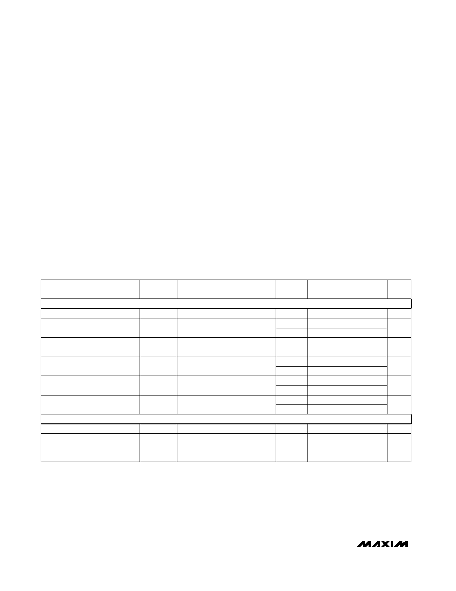
ABSOLUTE MAXIMUM RATINGS
ELECTRICAL CHARACTERISTICS—Dual Supplies
(V+ = +4.5V to +5.5V, V- = -4.5V to -5.5V, VINL = 0.8V, VINH = 2.4V, VGND = 0V, TA = TMIN to TMAX, unless otherwise noted. Typical
values are at TA = +25°C.)
Stresses beyond those listed under “Absolute Maximum Ratings” may cause permanent damage to the device. These are stress ratings only, and functional
operation of the device at these or any other conditions beyond those indicated in the operational sections of the specifications is not implied. Exposure to
absolute maximum rating conditions for extended periods may affect device reliability.
(Voltages referenced to GND)
V+ ...........................................................................-0.3V, +13.0V
V- ............................................................................-13.0V, +0.3V
V+ to V-...................................................................-0.3V, +13.0V
All Other Pins (Note 1) ..........................(V- - 0.3V) to (V+ + 0.3V)
Continuous Current into Any Terminal..............................±10mA
Peak Current into Any Terminal
(pulsed at 1ms, 10% duty cycle)..................................±50mA
ESD per Method 3015.7 ..................................................>2000V
Continuous Power Dissipation (TA = +70°C)
8-Pin Plastic DIP (derate 9.09mW/°C above +70°C) ...727mW
8-Pin SO (derate 5.88mW/°C above +70°C)............... 471mW
8-Pin MAX (derate 4.1mW/°C above +70°C) ............. 330mW
6-Pin SOT23-6 (derate 7.1mW/°C above +70°C) ........571mW
Operating Temperature Ranges
MAX4529C_ E .....................................................0°C to +70°C
MAX4529E_ E ..................................................-40°C to +85°C
Storage Temperature Range .............................-65°C to +150°C
Lead Temperature (soldering, 10s) .................................+300°C
Note 1: Voltages on all other pins exceeding V+ or V- are clamped by internal diodes. Limit forward diode current to maximum
current rating.
V+ = 5V, V- = -5V,
VCOM = ±3V, ICOM = 1mA
(Note 3)
V+ = 5.5V, V- = -5.5V,
VCOM = ±4.5V
V+ = 5V; V- = -5V; VCOM = 3V,
0V, -3V; ICOM = 1mA
V+ = 5.5V, V- = -5.5V,
VCOM = ±4.5V, VNC = 4.5V
V+ = 5.5V, V- = -5.5V,
VCOM = ±4.5V, VNC = 4.5V
VIN = 0.8V or 2.4V
CONDITIONS
A
-1
0.03
1
IINH, IINL
IN Input Current Logic High or
Low
45
70
RON
Signal-Path On-Resistance
V
V-
V+
VCOM, VNC
Analog Signal Range
V
0.8
1.5
VINL
IN Input Logic Threshold Low
V
1.5
2.4
VINH
IN Input Logic Threshold High
nA
-2
0.02
2
ICOM(ON)
COM On Leakage Current
(Notes 5, 6)
510
RFLAT(ON)
Signal-Path On-Resistance
Flatness (Note 4)
nA
-1
0.02
1
INC(OFF)
NC Off Leakage Current
(Notes 5, 6)
nA
-1
0.02
1
ICOM(OFF)
COM Off Leakage Current
(Notes 5, 6)
UNITS
MIN
TYP
MAX
(Note 2)
SYMBOL
PARAMETER
+25°C
C, E
+25°C
C, E
TA
C, E
-20
20
-20
20
-40
40
C, E
100
±
ANALOG SWITCH
LOGIC INPUT
±
相关PDF资料 |
PDF描述 |
|---|---|
| DF3068F25V | IC H8/3068F MCU FLASH 100QFP |
| MAX4528ESA | IC SWITCH DUAL SPDT 8SOIC |
| MAX4528CSA | IC SWITCH DUAL SPDT 8SOIC |
| MAX4527CUA | IC SWITCH DUAL SPDT 8UMAX |
| MAX4526EUA | IC SWITCH DUAL SPDT 8UMAX |
相关代理商/技术参数 |
参数描述 |
|---|---|
| MAX4529CSA | 功能描述:多路器开关 IC RoHS:否 制造商:Texas Instruments 通道数量:1 开关数量:4 开启电阻(最大值):7 Ohms 开启时间(最大值): 关闭时间(最大值): 传播延迟时间:0.25 ns 工作电源电压:2.3 V to 3.6 V 工作电源电流: 最大工作温度:+ 85 C 安装风格:SMD/SMT 封装 / 箱体:UQFN-16 |
| MAX4529CSA+ | 制造商:Maxim Integrated Products 功能描述: |
| MAX4529CSA-T | 功能描述:视频开关 IC RoHS:否 制造商:Texas Instruments 开关数量:4 开启电阻(最大值):12 Ohms 传播延迟时间: 开启时间(最大值): 关闭时间(最大值): 最大工作温度:+ 85 C 最小工作温度:- 40 C 封装 / 箱体:WQFN-42 封装:Reel |
| MAX4529CUA | 功能描述:多路器开关 IC RoHS:否 制造商:Texas Instruments 通道数量:1 开关数量:4 开启电阻(最大值):7 Ohms 开启时间(最大值): 关闭时间(最大值): 传播延迟时间:0.25 ns 工作电源电压:2.3 V to 3.6 V 工作电源电流: 最大工作温度:+ 85 C 安装风格:SMD/SMT 封装 / 箱体:UQFN-16 |
| MAX4529CUA-T | 功能描述:多路器开关 IC RoHS:否 制造商:Texas Instruments 通道数量:1 开关数量:4 开启电阻(最大值):7 Ohms 开启时间(最大值): 关闭时间(最大值): 传播延迟时间:0.25 ns 工作电源电压:2.3 V to 3.6 V 工作电源电流: 最大工作温度:+ 85 C 安装风格:SMD/SMT 封装 / 箱体:UQFN-16 |
发布紧急采购,3分钟左右您将得到回复。