- 您现在的位置:买卖IC网 > PDF目录11322 > MAX4533CPP+ (Maxim Integrated Products)IC SWITCH QUAD SPDT 20DIP PDF资料下载
参数资料
| 型号: | MAX4533CPP+ |
| 厂商: | Maxim Integrated Products |
| 文件页数: | 12/12页 |
| 文件大小: | 0K |
| 描述: | IC SWITCH QUAD SPDT 20DIP |
| 产品培训模块: | Lead (SnPb) Finish for COTS Obsolescence Mitigation Program |
| 标准包装: | 18 |
| 功能: | 开关 |
| 电路: | 4 x SPDT |
| 导通状态电阻: | 175 欧姆 |
| 电压电源: | 单/双电源 |
| 电压 - 电源,单路/双路(±): | 9 V ~ 36 V,±4.5 V ~ 18 V |
| 工作温度: | 0°C ~ 70°C |
| 安装类型: | 通孔 |
| 封装/外壳: | 20-DIP(0.300",7.62mm) |
| 供应商设备封装: | 20-PDIP |
| 包装: | 管件 |
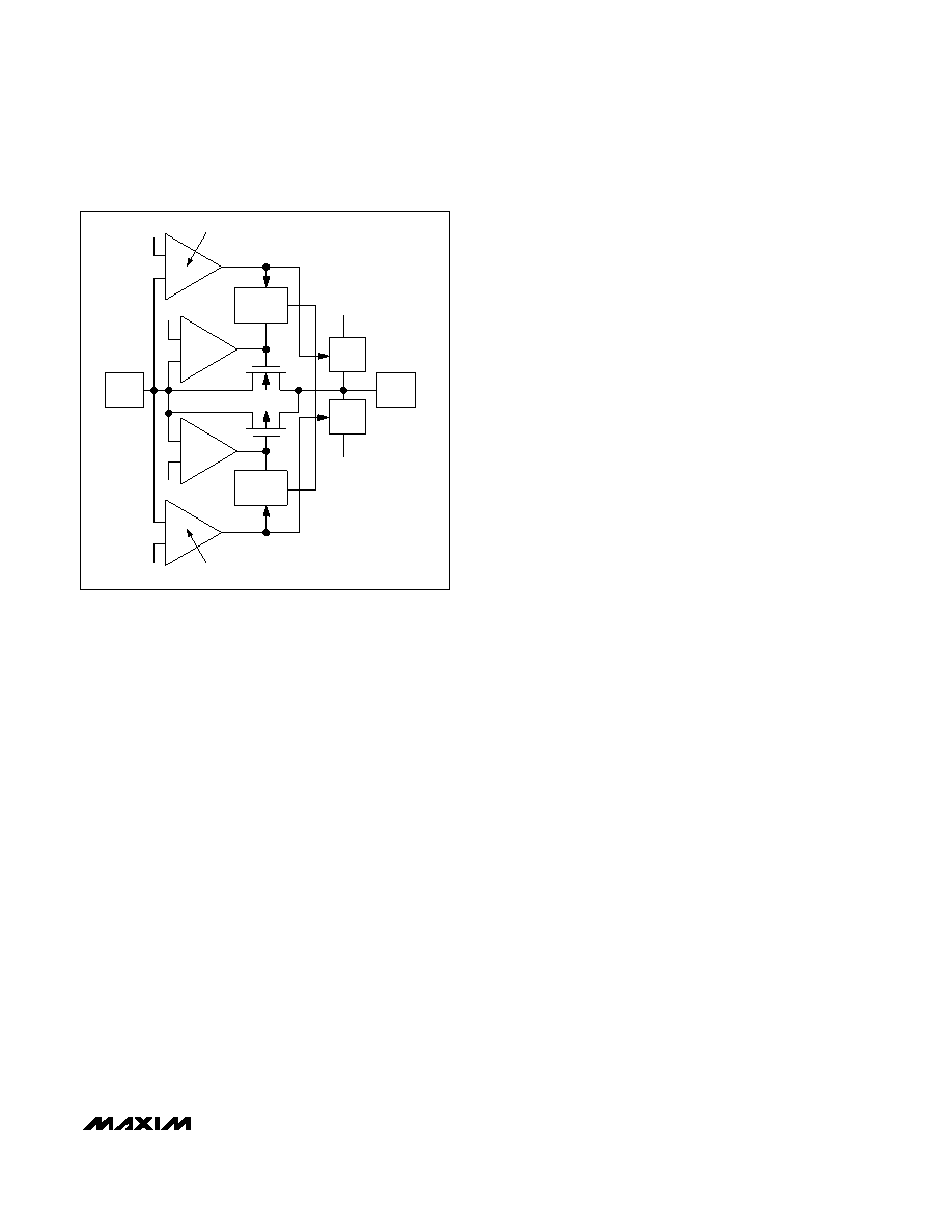
During normal operation of a conducting channel, N1
and P1 remain on with a typical 125
on-resistance
between NO_ (or NC_) and COM_. If the input voltage
exceeds either supply rail by about 150mV, the parallel
combination switches (N1, P1) are forced off through
the driver and sensing circuitries. At the same time, the
output (COM_ ) is clamped to the appropriate supply
rail by the clamp circuitries (N2, P2). Two clamp circuits
limit the output voltage to the supply voltages.
For simplicity, Figure 1 shows only one side of the SPDT
switch configuration. The complete circuit is composed
of two channels with their outputs connected.
Normal Operation
Two comparators continuously compare the voltage on
the NO_ (or NC_ ) pin with V+ and V- supply voltages.
When the signal on NO_ (or NC_ ) is between V+ and
V-, the switch behaves normally, with FETs N1 and P1
turning on and off in response to NO_ (or NC_) signals
(Figure 1). For any voltage between the supply rails,
the switch is bidirectional; therefore, COM_ and NC_
(or NO_ ) are interchangeable. Only NO_ and NC_ can
be exposed to overvoltages beyond the supply range
and within the specified breakdown limits of the device.
Fault Condition
The MAX4533 protects devices connected to its output
(COM_) through its unique fault-protection circuitry.
When the input voltage is raised above either supply
rail, the internal sense and comparator circuitries (N3
and N-channel driver or P3 and P-channel driver) dis-
connect the output (COM_) from the input (Figure 1).
If the switch driven above the supply rail has an on
state, the clamp circuitries (N2 or P2) connect the out-
put to the appropriate supply rail. Table 1 summarizes
the MAX4533’s operation under normal and fault condi-
tions. Row 5 shows a negative fault condition when the
supplies are on. It shows that with supplies of ±15V, if
the input voltage is between -15V and -25V, the output
(COM_) clamps to the negative supply rail of -15V.
With this technique, the SPDT switch is capable of with-
standing a worse-case condition of opposite fault polar-
ities at its inputs.
Transient Fault Condition
When a fast rising or falling transient on NO_ (or NC_)
exceeds V+ or V-, the output (COM_) follows the input
(IN_) to the supply rail by only a few nanoseconds. This
delay is due to the switch on-resistance and circuit
capacitance to ground. However, when the input tran-
sient returns to within the supply rails there is a longer
recovery time. For positive faults, the recovery time is
typically 2.5s. For negative faults, the recovery time is
typically 1.3s. These values depend on the COM_ out-
put resistance and capacitance. The delays are not
dependent on the fault amplitude. Higher COM_ output
resistance and capacitance increase the recovery
times.
Fault Protection, Voltage, and Power Off
The maximum fault voltage on the NO_ or NC_ pins is
±40V from ground when the power is off. With ±15V sup-
ply voltages, the highest voltage on NO_ (or NC_) can
be +25V, and the lowest voltage on NO_ (or NC_) can
be -25V. Exceeding these limits can damage the chip.
IN_ Logic-Level Thresholds
The logic-level thresholds are TTL/CMOS-compatible
when V+ is +15V. Raising V+ increases the threshold
slightly; when V+ reaches +25V, the level threshold is
2.8V—higher than the TTL output high-level minimum of
2.4V, but still compatible with CMOS outputs (see the
Typical Operating Characteristics).
Increasing V- has no effect on the logic-level thresh-
olds, but it does increase the gate-drive voltage to the
signal FETs, reducing their on-resistance.
MAX4533
Quad, Rail-to-Rail, Fault-Protected,
SPDT Analog Switch
_______________________________________________________________________________________
9
-15V
+15V
P-CHANNEL
DRIVER
N-CHANNEL
DRIVER
+15V
N3
P3
INPUT
NC_
or
NO_
N1
CLAMP
OUTPUT COM_
CLAMP
+V(+15V)
-V(-15V)
N2
P2
P1
COMPARATOR
SENSE
SWITCH
SENSE
SWITCH
Figure 1. Simplified Internal Structure
相关PDF资料 |
PDF描述 |
|---|---|
| VE-JTH-IX-F3 | CONVERTER MOD DC/DC 52V 75W |
| MAX4711EUE+ | IC SWITCH QUAD SPST 16TSSOP |
| VE-JTH-IX-F2 | CONVERTER MOD DC/DC 52V 75W |
| MAX301CSE+ | IC SWITCH DUAL SPST 16SOIC |
| MAX4558ESE+ | IC MULTIPLEXER 8X1 16SOIC |
相关代理商/技术参数 |
参数描述 |
|---|---|
| MAX4533CPP+ | 功能描述:模拟开关 IC Quad Fault-Protected SPDT Analog Switch RoHS:否 制造商:Texas Instruments 开关数量:2 开关配置:SPDT 开启电阻(最大值):0.1 Ohms 切换电压(最大): 开启时间(最大值): 关闭时间(最大值): 工作电源电压:2.7 V to 4.5 V 最大工作温度:+ 85 C 安装风格:SMD/SMT 封装 / 箱体:DSBGA-16 |
| MAX4533CWP | 功能描述:模拟开关 IC RoHS:否 制造商:Texas Instruments 开关数量:2 开关配置:SPDT 开启电阻(最大值):0.1 Ohms 切换电压(最大): 开启时间(最大值): 关闭时间(最大值): 工作电源电压:2.7 V to 4.5 V 最大工作温度:+ 85 C 安装风格:SMD/SMT 封装 / 箱体:DSBGA-16 |
| MAX4533CWP+ | 功能描述:模拟开关 IC Quad Fault-Protected SPDT Analog Switch RoHS:否 制造商:Texas Instruments 开关数量:2 开关配置:SPDT 开启电阻(最大值):0.1 Ohms 切换电压(最大): 开启时间(最大值): 关闭时间(最大值): 工作电源电压:2.7 V to 4.5 V 最大工作温度:+ 85 C 安装风格:SMD/SMT 封装 / 箱体:DSBGA-16 |
| MAX4533CWP+T | 功能描述:模拟开关 IC Quad Fault-Protected SPDT Analog Switch RoHS:否 制造商:Texas Instruments 开关数量:2 开关配置:SPDT 开启电阻(最大值):0.1 Ohms 切换电压(最大): 开启时间(最大值): 关闭时间(最大值): 工作电源电压:2.7 V to 4.5 V 最大工作温度:+ 85 C 安装风格:SMD/SMT 封装 / 箱体:DSBGA-16 |
| MAX4533CWP-T | 功能描述:模拟开关 IC RoHS:否 制造商:Texas Instruments 开关数量:2 开关配置:SPDT 开启电阻(最大值):0.1 Ohms 切换电压(最大): 开启时间(最大值): 关闭时间(最大值): 工作电源电压:2.7 V to 4.5 V 最大工作温度:+ 85 C 安装风格:SMD/SMT 封装 / 箱体:DSBGA-16 |
发布紧急采购,3分钟左右您将得到回复。