- 您现在的位置:买卖IC网 > PDF目录11159 > MAX4581LEEE+ (Maxim Integrated Products)IC MULTIPLEXER 8X1 16QSOP PDF资料下载
参数资料
| 型号: | MAX4581LEEE+ |
| 厂商: | Maxim Integrated Products |
| 文件页数: | 14/16页 |
| 文件大小: | 0K |
| 描述: | IC MULTIPLEXER 8X1 16QSOP |
| 产品培训模块: | Lead (SnPb) Finish for COTS Obsolescence Mitigation Program |
| 标准包装: | 100 |
| 功能: | 多路复用器 |
| 电路: | 1 x 8:1 |
| 导通状态电阻: | 80 欧姆 |
| 电压电源: | 单/双电源 |
| 电压 - 电源,单路/双路(±): | 2 V ~ 12 V,±2 V ~ 6 V |
| 电流 - 电源: | 1µA |
| 工作温度: | -40°C ~ 85°C |
| 安装类型: | 表面贴装 |
| 封装/外壳: | 16-SSOP(0.154",3.90mm 宽) |
| 供应商设备封装: | 16-QSOP |
| 包装: | 管件 |
MAX4581L/MAX4582L/MAX4583L
Low-Voltage, CMOS Analog
Multiplexers/Switches
_______________________________________________________________________________________
7
Detailed Description
The MAX4581L/MAX4582L/MAX4583L are low-voltage,
CMOS analog ICs that operate from a single supply of
+2V to +12V. The MAX4581L is configured as an 8-
channel multiplexer, the MAX4582L as two 4-channel
multiplexers, and the MAX4583L as three single-
pole/double-throw (SPDT) switches. These devices can
handle rail-to-rail analog signals with only 2nA of off-
leakage current at +25°C.
The MAX4581L/MAX4582L/MAX4583L are TTL/CMOS-
logic compatible with 0.8V to 2.0V logic thresholds for
all digital inputs when operating from a +12V supply.
Applications Information
Power-Supply Considerations
The MAX4581L/MAX4582L/MAX4583Ls’ construction is
typical of most CMOS analog switches. The supply
input, VCC, is used to power the internal CMOS switch-
es and sets the limit of the analog voltage on any
switch. Reverse ESD protection diodes are internally
connected between each analog signal pin and both
VCC and GND. If any analog signal exceeds VCC or
goes below GND, one of these diodes conducts.
During normal operation, these reverse-biased ESD
diodes leak, causing the only current drawn from VCC
or GND. Virtually all the analog leakage current comes
from the ESD diodes. Although the ESD diodes on a
given signal pin are identical, and therefore fairly well
balanced, they are reverse biased differently by either
VCC or GND and the analog signal. This means that
leakage varies as the analog signal varies. The differ-
ence in the two diodes’ leakage to VCC and GND con-
stitutes the analog signal-path leakage current.
Because there is no connection between the analog
signal paths and GND, all analog leakage current flows
between each pin and one of the supply terminals, not
to the other switch terminal. Because of this, both sides
of a given switch can show leakage currents of either
the same or opposite polarity.
VCC and GND power the internal logic and logic-level
translators, and set both the input and output logic lim-
its. The logic-level translators convert the logic levels
into switched VCC and GND signals to drive the gates
of the analog switches. This drive signal is the only
connection between the logic supplies (and signals)
and the analog supplies. The logic-level thresholds are
TTL/CMOS compatible when VCC is +12V.
Overvoltage Protection
Proper power-supply sequencing is recommended for
all CMOS devices. Do not exceed the absolute maxi-
mum ratings because stresses beyond the listed rat-
ings can cause permanent damage to the devices.
Always sequence VCC first, followed by the logic inputs
and analog signals.
Pin Nomenclature
The MAX4581L/MAX4582L/MAX4583L are pin compati-
ble with the industry-standard 74HC4051/74HC4052/
74HC4053 and the MAX4051/MAX4052/MAX4053.
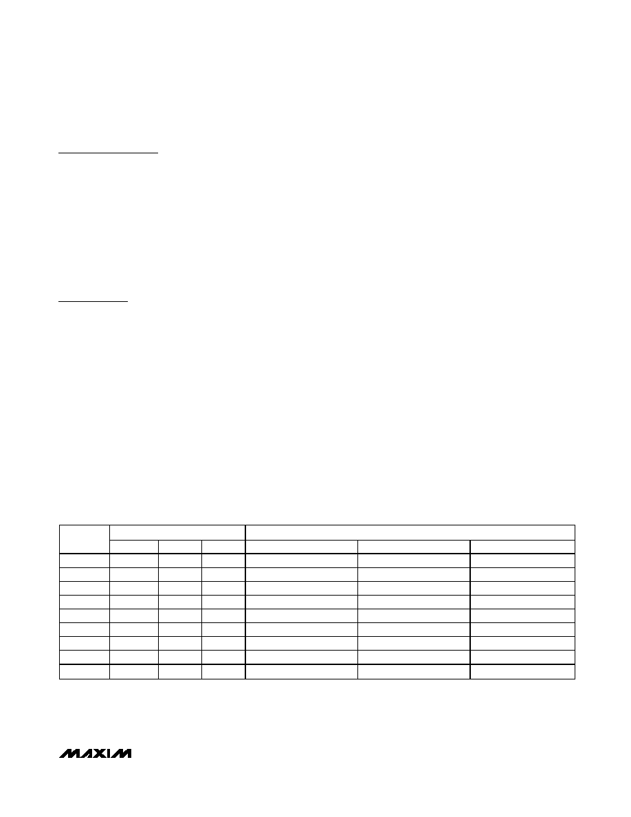
Table 1. Truth Table/Switch Programming
SELECT INPUTS
ON SWITCHES
ENABLE
INPUT
C*
B
A
MAX4581L
MAX4582L
MAX4583L
H
X
All switches open
L
X–X0
X–X0, Y–Y0
X–X0, Y–Y0, Z–Z0
L
H
X–X1
X–X1, Y–Y1
X–X1, Y–Y0, Z–Z0
L
H
L
X–X2
X–X2, Y–Y2
X–X0, Y–Y1, Z–Z0
L
H
X–X3
X–X3, Y–Y3
X–X1, Y–Y1, Z–Z0
L
H
L
X–X4
X–X0, Y–Y0
X–X0, Y–Y0, Z–Z1
L
H
L
H
X–X5
X–X1, Y–Y1
X–X1, Y–Y0, Z–Z1
L
H
L
X–X6
X–X2, Y–Y2
X–X0, Y–Y1, Z–Z1
L
H
X–X7
X–X3, Y-Y3
X–X1, Y–Y1, Z–Z1
X = Don’t care.
*C not present on MAX4582L.
Note: Input and output pins are identical and interchangeable. Either may be considered an input or output; signals pass equally
well in either direction.
相关PDF资料 |
PDF描述 |
|---|---|
| MAX4581LESE+ | IC MULTIPLEXER 8X1 16SOIC |
| MAX4583LEEE+ | IC SWITCH TRIPLE SPDT 16QSOP |
| MAX4582LESE+ | IC MULTIPLEXER DUAL 4X1 16SOIC |
| MAX4583LESE+ | IC SWITCH TRIPLE SPDT 16SOIC |
| MAX4522EPE+ | IC SWITCH QUAD SPST 16DIP |
相关代理商/技术参数 |
参数描述 |
|---|---|
| MAX4581LEEE+ | 功能描述:多路器开关 IC 8:1 Low Voltage Analog MUX RoHS:否 制造商:Texas Instruments 通道数量:1 开关数量:4 开启电阻(最大值):7 Ohms 开启时间(最大值): 关闭时间(最大值): 传播延迟时间:0.25 ns 工作电源电压:2.3 V to 3.6 V 工作电源电流: 最大工作温度:+ 85 C 安装风格:SMD/SMT 封装 / 箱体:UQFN-16 |
| MAX4581LEEE+T | 功能描述:多路器开关 IC 8:1 Low Voltage Analog MUX RoHS:否 制造商:Texas Instruments 通道数量:1 开关数量:4 开启电阻(最大值):7 Ohms 开启时间(最大值): 关闭时间(最大值): 传播延迟时间:0.25 ns 工作电源电压:2.3 V to 3.6 V 工作电源电流: 最大工作温度:+ 85 C 安装风格:SMD/SMT 封装 / 箱体:UQFN-16 |
| MAX4581LEEE-T | 功能描述:多路器开关 IC RoHS:否 制造商:Texas Instruments 通道数量:1 开关数量:4 开启电阻(最大值):7 Ohms 开启时间(最大值): 关闭时间(最大值): 传播延迟时间:0.25 ns 工作电源电压:2.3 V to 3.6 V 工作电源电流: 最大工作温度:+ 85 C 安装风格:SMD/SMT 封装 / 箱体:UQFN-16 |
| MAX4581LESE | 功能描述:多路器开关 IC RoHS:否 制造商:Texas Instruments 通道数量:1 开关数量:4 开启电阻(最大值):7 Ohms 开启时间(最大值): 关闭时间(最大值): 传播延迟时间:0.25 ns 工作电源电压:2.3 V to 3.6 V 工作电源电流: 最大工作温度:+ 85 C 安装风格:SMD/SMT 封装 / 箱体:UQFN-16 |
| MAX4581LESE+ | 功能描述:多路器开关 IC 8:1 Low Voltage Analog MUX RoHS:否 制造商:Texas Instruments 通道数量:1 开关数量:4 开启电阻(最大值):7 Ohms 开启时间(最大值): 关闭时间(最大值): 传播延迟时间:0.25 ns 工作电源电压:2.3 V to 3.6 V 工作电源电流: 最大工作温度:+ 85 C 安装风格:SMD/SMT 封装 / 箱体:UQFN-16 |
发布紧急采购,3分钟左右您将得到回复。