- 您现在的位置:买卖IC网 > PDF目录11155 > MAX4583AUE+T (Maxim Integrated Products)IC SWITCH TRIPLE SPDT 16TSSOP PDF资料下载
参数资料
| 型号: | MAX4583AUE+T |
| 厂商: | Maxim Integrated Products |
| 文件页数: | 17/17页 |
| 文件大小: | 0K |
| 描述: | IC SWITCH TRIPLE SPDT 16TSSOP |
| 产品培训模块: | Lead (SnPb) Finish for COTS Obsolescence Mitigation Program |
| 标准包装: | 2,500 |
| 功能: | 开关 |
| 电路: | 3 x SPDT |
| 导通状态电阻: | 80 欧姆 |
| 电压电源: | 单/双电源 |
| 电压 - 电源,单路/双路(±): | 2 V ~ 12 V,±2 V ~ 6 V |
| 电流 - 电源: | 1µA |
| 工作温度: | -40°C ~ 125°C |
| 安装类型: | 表面贴装 |
| 封装/外壳: | 16-TSSOP(0.173",4.40mm 宽) |
| 供应商设备封装: | 16-TSSOP |
| 包装: | 带卷 (TR) |
MAX4581/MAX4582/MAX4583
Low-Voltage, CMOS Analog
Multiplexers/Switches
_______________________________________________________________________________________
9
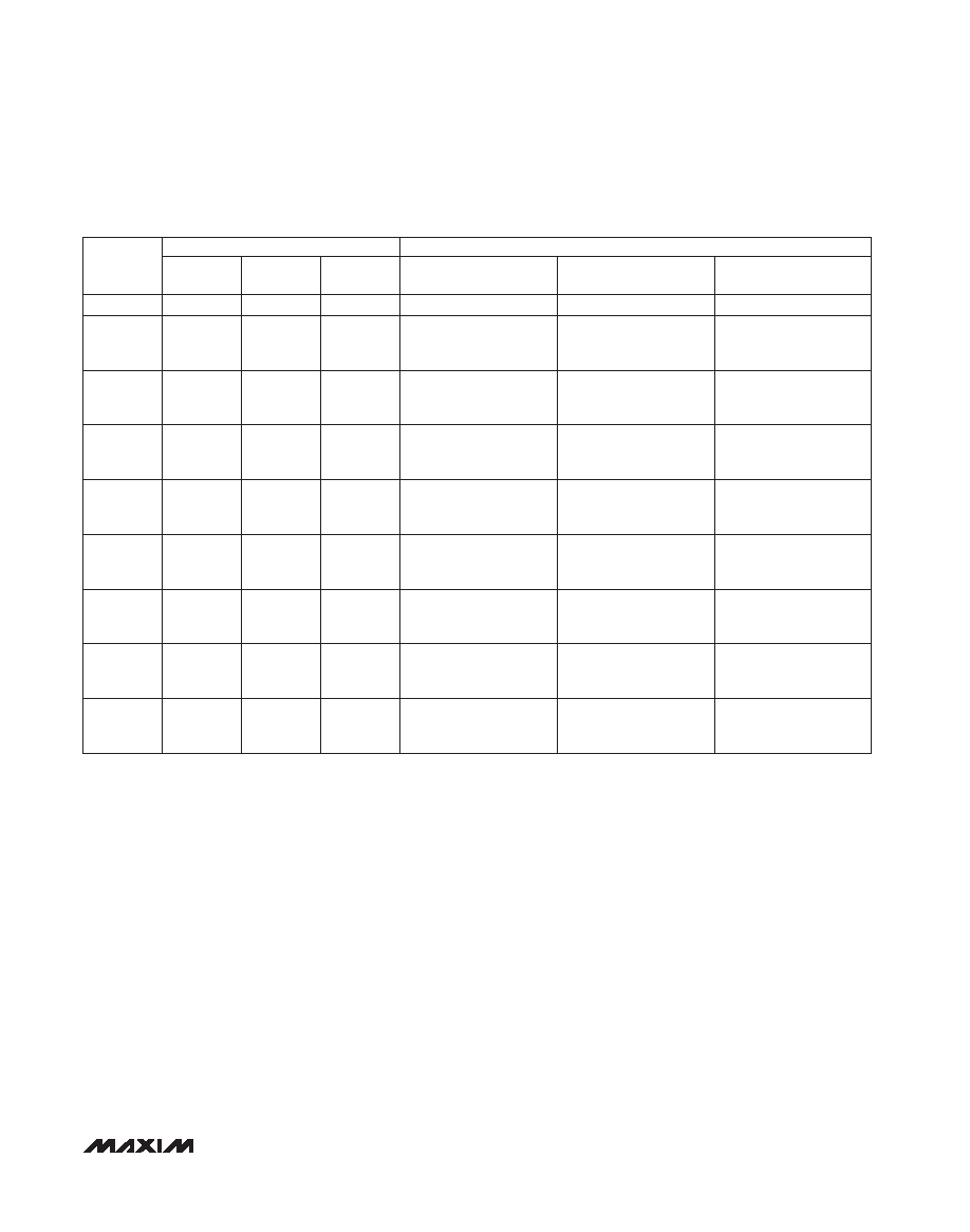
X
H
Table 1. Truth Table/Switch Programming
X
All switches open
L
X–X0
X–X0,
Y–Y0
X–X0,
Y–Y0,
Z–Z0
L
H
X–X1
X–X1,
Y–Y1
X–X1,
Y–Y0,
Z–Z0
L
H
X–X3
X–X3,
Y–Y3
X–X1,
Y–Y1,
Z–Z0
H
L
X–X2
X–X2,
Y–Y2
X–X0,
Y–Y1,
Z–Z0
L
H
X–X5
X–X1,
Y–Y1
X–X1,
Y–Y0,
Z–Z1
L
X–X4
X–X0,
Y–Y0
X–X0,
Y–Y0,
Z–Z1
H
L
H
L
H
X–X7
X–X3,
Y–Y3
X–X1,
Y–Y1,
Z–Z1
H
L
X–X6
X–X2,
Y–Y2
X–X0,
Y–Y1,
Z–Z1
H
L
H
L
X = Don’t care
*
C not present on MAX4582.
Note: Input and output pins are identical and interchangeable. Either may be considered an input or output; signals pass equally
well in either direction.
ON SWITCHES
SELECT INPUTS
B
A
MAX4581
MAX4582
MAX4583
C*
ENABLE
INPUT
will conduct. During normal operation, these and other
reverse-biased ESD diodes leak, forming the only cur-
rent drawn from VCC or VEE.
Virtually all the analog leakage current comes from the
ESD diodes. Although the ESD diodes on a given sig-
nal pin are identical and therefore fairly well balanced,
they are reverse biased differently. Each is biased by
either VCC or VEE and the analog signal. This means
their leakages will vary as the signal varies. The
differ-
ence in the two diode leakages to the VCC and VEE
pins constitutes the analog-signal-path leakage current.
All analog leakage current flows between each pin and
one of the supply terminals, not to the other switch ter-
minal. This is why both sides of a given switch can
show leakage currents of either the same or opposite
polarity.
There is no connection between the analog-signal
paths and GND.
VCC and GND power the internal logic and logic-level
translators, and set the input logic limits. The logic-level
translators convert the logic levels into switched VCC
and VEE signals to drive the gates of the analog sig-
nals. This drive signal is the only connection between
the logic supplies and signals and the analog supplies.
VCC and VEE have ESD-protection diodes to GND.
The logic-level thresholds are TTL/CMOS compatible
when VCC is +5V. As VCC rises, the threshold increases
相关PDF资料 |
PDF描述 |
|---|---|
| MAX4909EBC+T | IC MULTIPLEXER DUAL 3X1 12UCSP |
| MAX4066CSD+T | IC SWITCH QUAD SPST 14SOIC |
| MAX4797ETT+T | IC SWITCH 1X1 6TDFN |
| MAX4720ELT+T | IC SWITCH 6UDFN |
| MAX4720ELT+TG104 | IC SWITCH 6UDFN |
相关代理商/技术参数 |
参数描述 |
|---|---|
| MAX4583C/D | 功能描述:模拟开关 IC RoHS:否 制造商:Texas Instruments 开关数量:2 开关配置:SPDT 开启电阻(最大值):0.1 Ohms 切换电压(最大): 开启时间(最大值): 关闭时间(最大值): 工作电源电压:2.7 V to 4.5 V 最大工作温度:+ 85 C 安装风格:SMD/SMT 封装 / 箱体:DSBGA-16 |
| MAX4583C/D DIE | 制造商:Maxim Integrated Products 功能描述: |
| MAX4583CEE | 功能描述:模拟开关 IC RoHS:否 制造商:Texas Instruments 开关数量:2 开关配置:SPDT 开启电阻(最大值):0.1 Ohms 切换电压(最大): 开启时间(最大值): 关闭时间(最大值): 工作电源电压:2.7 V to 4.5 V 最大工作温度:+ 85 C 安装风格:SMD/SMT 封装 / 箱体:DSBGA-16 |
| MAX4583CEE+ | 功能描述:模拟开关 IC 3Ch SPDT Low V Analog Switch RoHS:否 制造商:Texas Instruments 开关数量:2 开关配置:SPDT 开启电阻(最大值):0.1 Ohms 切换电压(最大): 开启时间(最大值): 关闭时间(最大值): 工作电源电压:2.7 V to 4.5 V 最大工作温度:+ 85 C 安装风格:SMD/SMT 封装 / 箱体:DSBGA-16 |
| MAX4583CEE+T | 功能描述:模拟开关 IC 3Ch SPDT Low V Analog Switch RoHS:否 制造商:Texas Instruments 开关数量:2 开关配置:SPDT 开启电阻(最大值):0.1 Ohms 切换电压(最大): 开启时间(最大值): 关闭时间(最大值): 工作电源电压:2.7 V to 4.5 V 最大工作温度:+ 85 C 安装风格:SMD/SMT 封装 / 箱体:DSBGA-16 |
发布紧急采购,3分钟左右您将得到回复。