- 您现在的位置:买卖IC网 > PDF目录11158 > MAX4612CUD+T (Maxim Integrated Products)IC SWITCH QUAD SPST 14TSSOP PDF资料下载
参数资料
| 型号: | MAX4612CUD+T |
| 厂商: | Maxim Integrated Products |
| 文件页数: | 9/11页 |
| 文件大小: | 0K |
| 描述: | IC SWITCH QUAD SPST 14TSSOP |
| 产品培训模块: | Lead (SnPb) Finish for COTS Obsolescence Mitigation Program |
| 标准包装: | 2,500 |
| 功能: | 开关 |
| 电路: | 4 x SPST - NC/NO |
| 导通状态电阻: | 100 欧姆 |
| 电压电源: | 单电源 |
| 电压 - 电源,单路/双路(±): | 2 V ~ 12 V |
| 电流 - 电源: | 1µA |
| 工作温度: | 0°C ~ 70°C |
| 安装类型: | 表面贴装 |
| 封装/外壳: | 14-TSSOP(0.173",4.40mm 宽) |
| 供应商设备封装: | 14-TSSOP |
| 包装: | 带卷 (TR) |
Applications Information
Power-Supply Sequencing
and Overvoltage Protection
Do not exceed the absolute maximum ratings, because
stresses beyond the listed ratings may cause permanent
damage to the devices.
Proper power-supply sequencing is recommended for all
CMOS devices. Always apply V+ before applying analog
signals or logic inputs, especially if the analog or logic
signals are not current limited. If this sequencing is not
possible, and if the analog or logic inputs are not current
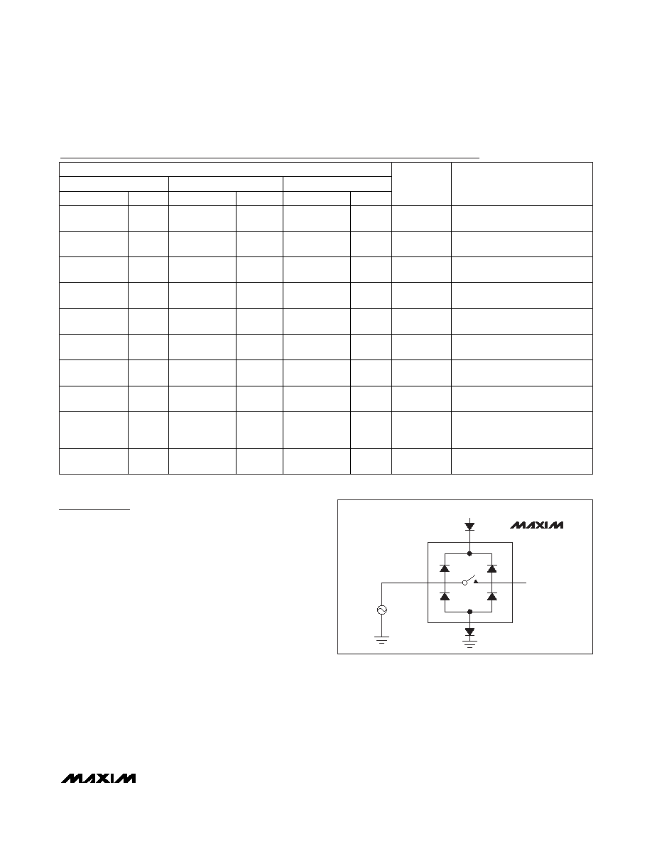
limited to 20mA, add a small-signal diode (D1) as shown
in Figure 1. If the analog signal can dip below GND, add
D2. Adding protection diodes reduces the analog signal
range to a diode drop (about 0.7V) below V+ (for D1),
and to a diode drop above ground (for D2). Leakage is
unaffected by adding the diodes. On-resistance increas-
es by a small amount at low supply voltages. Maximum
supply voltage (V+) must not exceed 13V.
Adding protection diodes causes the logic thresholds to
be shifted relative to the power-supply rails. This can be
significant when low supply voltages (+5V or less) are
used. With a +5V supply, TTL compatibility is not guar-
anteed when protection diodes are added. Driving IN1
and IN2 all the way to the supply rails (i.e., to a diode
drop higher than the V+ pin, or to a diode drop lower
than the GND pin) is always acceptable.
MAX4610/MAX4611/MAX4612
Low-Voltage, Quad, SPST
CMOS Analog Switches
_______________________________________________________________________________________
7
POSITIVE SUPPLY
COM_
NO_
Vg
V+
MAX4610
MAX4611
MAX4612
Figure 1. Overvoltage Protection Using Two External Blocking
Diodes
Pin Description
PIN
MAX4610
MAX4611
MAX4612
TSSOP/SO/ DIP
QFN
TSSOP/SO/DIP
QFN
TSSOP/SO/DIP
QFN
NAME
FUNCTION
1, 3, 8, 11
1, 3,
8, 11
—
NO1–NO4
Analog Switch Normally Open
Terminals
—
1, 3, 8, 11
1, 3,
8, 11
—
NC1–NC4
Analog Switch Normally Closed
Terminals
—
1, 8
NO1, NO3
Analog Switch Normally Open
Terminals
—
3, 11
NC2, NC4
Analog Switch Normally Closed
Terminals
2, 4, 9, 10
2, 4,
9, 10
2, 4, 9, 10
2, 4,
9, 10
2, 4, 9, 10
2, 4,
9, 10
COM1–COM4
Analog Switch Common
Terminals
13, 5, 6, 12
14, 5,
6, 13
13, 5, 6, 12
14, 5,
6, 13
13, 5, 6, 12
14, 5,
6, 13
IN1–IN4
Logic-Control Digital Input
7
GND
Ground. Connect to digital
ground.
—
12, 15
—
12, 15
—
12, 15
N.C.
No Connection. Not internally
connected.
14
16
14
16
14
16
V+
Positive Analog and Digital-
Supply Voltage Input. Internally
connected to substrate.
—
EP
Exposed Pad (QFN only).
Connect to V+.
相关PDF资料 |
PDF描述 |
|---|---|
| EFM32TG230F16 | MCU 32BIT 16KB FLASH 64-QFN |
| MAX4522CUE+T | IC SWITCH QUAD SPST 16TSSOP |
| MAX4723EUA+T | IC SWITCH DUAL SPST 8UMAX |
| C8051F713-GQ | IC 8051 MCU 8K FLASH 48-TQFP |
| MAX4722EUA+T | IC SWITCH DUAL SPST 8UMAX |
相关代理商/技术参数 |
参数描述 |
|---|---|
| MAX4612EPD | 功能描述:模拟开关 IC RoHS:否 制造商:Texas Instruments 开关数量:2 开关配置:SPDT 开启电阻(最大值):0.1 Ohms 切换电压(最大): 开启时间(最大值): 关闭时间(最大值): 工作电源电压:2.7 V to 4.5 V 最大工作温度:+ 85 C 安装风格:SMD/SMT 封装 / 箱体:DSBGA-16 |
| MAX4612ESD | 功能描述:模拟开关 IC RoHS:否 制造商:Texas Instruments 开关数量:2 开关配置:SPDT 开启电阻(最大值):0.1 Ohms 切换电压(最大): 开启时间(最大值): 关闭时间(最大值): 工作电源电压:2.7 V to 4.5 V 最大工作温度:+ 85 C 安装风格:SMD/SMT 封装 / 箱体:DSBGA-16 |
| MAX4612ESD+ | 功能描述:模拟开关 IC Quad SPST CMOS Analog Switch RoHS:否 制造商:Texas Instruments 开关数量:2 开关配置:SPDT 开启电阻(最大值):0.1 Ohms 切换电压(最大): 开启时间(最大值): 关闭时间(最大值): 工作电源电压:2.7 V to 4.5 V 最大工作温度:+ 85 C 安装风格:SMD/SMT 封装 / 箱体:DSBGA-16 |
| MAX4612ESD+T | 功能描述:模拟开关 IC Quad SPST CMOS Analog Switch RoHS:否 制造商:Texas Instruments 开关数量:2 开关配置:SPDT 开启电阻(最大值):0.1 Ohms 切换电压(最大): 开启时间(最大值): 关闭时间(最大值): 工作电源电压:2.7 V to 4.5 V 最大工作温度:+ 85 C 安装风格:SMD/SMT 封装 / 箱体:DSBGA-16 |
| MAX4612ESD-T | 功能描述:模拟开关 IC RoHS:否 制造商:Texas Instruments 开关数量:2 开关配置:SPDT 开启电阻(最大值):0.1 Ohms 切换电压(最大): 开启时间(最大值): 关闭时间(最大值): 工作电源电压:2.7 V to 4.5 V 最大工作温度:+ 85 C 安装风格:SMD/SMT 封装 / 箱体:DSBGA-16 |
发布紧急采购,3分钟左右您将得到回复。