- 您现在的位置:买卖IC网 > PDF目录11043 > MAX4616CPD (Maxim Integrated Products)IC SWITCH QUAD SPST 14DIP PDF资料下载
参数资料
| 型号: | MAX4616CPD |
| 厂商: | Maxim Integrated Products |
| 文件页数: | 11/12页 |
| 文件大小: | 0K |
| 描述: | IC SWITCH QUAD SPST 14DIP |
| 产品培训模块: | Lead (SnPb) Finish for COTS Obsolescence Mitigation Program |
| 标准包装: | 25 |
| 功能: | 开关 |
| 电路: | 4 x SPST - NC/NO |
| 导通状态电阻: | 10 欧姆 |
| 电压电源: | 单电源 |
| 电压 - 电源,单路/双路(±): | 2 V ~ 5.5 V |
| 电流 - 电源: | 1µA |
| 工作温度: | 0°C ~ 70°C |
| 安装类型: | 通孔 |
| 封装/外壳: | 14-DIP(0.300",7.62mm) |
| 供应商设备封装: | 14-PDIP |
| 包装: | 管件 |
MAX4614/MAX4615/MAX4616
Low-Voltage, High-Speed, Quad, SPST
CMOS Analog Switches
8
_______________________________________________________________________________________
Applications Information
Power-Supply Sequencing and
Overvoltage Protection
Do not exceed the absolute maximum ratings because
stresses beyond the listed ratings may cause perma-
nent damage to the devices.
Proper power-supply sequencing is recommended for
all CMOS devices. Always apply V+ before applying
analog signals or logic inputs, especially if the analog
or logic signals are not current limited. If this sequenc-
ing is not possible, and if the analog or logic inputs are
not current limited to 20mA, add a small-signal diode
(D1) as shown in Figure 1. If the analog signal can dip
below GND, add D2. Adding protection diodes
reduces the analog signal range to a diode drop (about
0.7V) below V+ (for D1), and to a diode drop above
ground (for D2). Leakage is unaffected by adding the
diodes. On-resistance increases by a small amount at
low supply voltages. Maximum supply voltage (V+)
must not exceed 6V.
Adding protection diodes causes the logic thresholds
to be shifted relative to the power-supply rails. This can
be significant when low supply voltages (+5V or less)
are used. With a +5V supply, TTL compatibility is not
guaranteed when protection diodes are added. Driving
IN1 and IN2 all the way to the supply rails (i.e., to a
diode drop higher than the V+ pin, or to a diode drop
lower than the GND pin) is always acceptable.
Protection diodes D1 and D2 also protect against some
overvoltage situations. With Figure 1’s circuit, if the sup-
ply voltage is below the absolute maximum rating, and
if a fault voltage up to the absolute maximum rating is
applied to an analog signal pin, no damage will result.
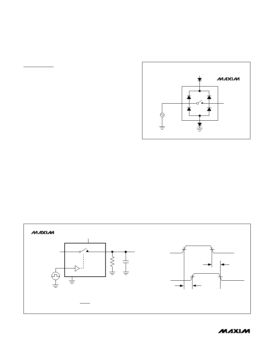
POSITIVE SUPPLY
COM_
NO_
Vg
V+
D1
D2
MAX4614
MAX4615
MAX4616
Figure 1. Overvoltage Protection Using Two External Blocking
Diodes
tR < 20ns
tF < 20ns
50%
0
LOGIC
INPUT
RL
300
NO_, NC_
GND
CL INCLUDES FIXTURE AND STRAY CAPACITANCE.
VOUT = VCOM
(
RL
)
RL + RON
SWITCH
INPUT
IN_
VINH
tOFF
0
COM_
SWITCH
OUTPUT
0.9
V0UT
0.9
VOUT
tON
VOUT
SWITCH
OUTPUT
LOGIC
INPUT
V+
CL
35pF
V+
VOUT
VCOM_
MAX4614
MAX4615
MAX4616
Figure 2. Switching Time
______________________________________________Test Circuits/Timing Diagrams
相关PDF资料 |
PDF描述 |
|---|---|
| MAX4615ESD | IC SWITCH QUAD SPST 14SOIC |
| MAX4615CSD | IC SWITCH QUAD SPST 14SOIC |
| MAX4614EUD | IC SWITCH QUAD SPST 14TSSOP |
| MAX4614ESD | IC SWITCH QUAD SPST 14SOIC |
| MAX4614EPD | IC SWITCH QUAD SPST 14DIP |
相关代理商/技术参数 |
参数描述 |
|---|---|
| MAX4616CPD+ | 功能描述:模拟开关 IC Quad SPST Analog Switch RoHS:否 制造商:Texas Instruments 开关数量:2 开关配置:SPDT 开启电阻(最大值):0.1 Ohms 切换电压(最大): 开启时间(最大值): 关闭时间(最大值): 工作电源电压:2.7 V to 4.5 V 最大工作温度:+ 85 C 安装风格:SMD/SMT 封装 / 箱体:DSBGA-16 |
| MAX4616CSD | 功能描述:模拟开关 IC RoHS:否 制造商:Texas Instruments 开关数量:2 开关配置:SPDT 开启电阻(最大值):0.1 Ohms 切换电压(最大): 开启时间(最大值): 关闭时间(最大值): 工作电源电压:2.7 V to 4.5 V 最大工作温度:+ 85 C 安装风格:SMD/SMT 封装 / 箱体:DSBGA-16 |
| MAX4616CSD+ | 功能描述:模拟开关 IC Quad SPST Analog Switch RoHS:否 制造商:Texas Instruments 开关数量:2 开关配置:SPDT 开启电阻(最大值):0.1 Ohms 切换电压(最大): 开启时间(最大值): 关闭时间(最大值): 工作电源电压:2.7 V to 4.5 V 最大工作温度:+ 85 C 安装风格:SMD/SMT 封装 / 箱体:DSBGA-16 |
| MAX4616CSD+T | 功能描述:模拟开关 IC Quad SPST Analog Switch RoHS:否 制造商:Texas Instruments 开关数量:2 开关配置:SPDT 开启电阻(最大值):0.1 Ohms 切换电压(最大): 开启时间(最大值): 关闭时间(最大值): 工作电源电压:2.7 V to 4.5 V 最大工作温度:+ 85 C 安装风格:SMD/SMT 封装 / 箱体:DSBGA-16 |
| MAX4616CSD-T | 功能描述:模拟开关 IC RoHS:否 制造商:Texas Instruments 开关数量:2 开关配置:SPDT 开启电阻(最大值):0.1 Ohms 切换电压(最大): 开启时间(最大值): 关闭时间(最大值): 工作电源电压:2.7 V to 4.5 V 最大工作温度:+ 85 C 安装风格:SMD/SMT 封装 / 箱体:DSBGA-16 |
发布紧急采购,3分钟左右您将得到回复。