- 您现在的位置:买卖IC网 > PDF目录1942 > MAX4633ESE+T (Maxim Integrated Products)IC SWITCH DUAL DPST 16SOIC PDF资料下载
参数资料
| 型号: | MAX4633ESE+T |
| 厂商: | Maxim Integrated Products |
| 文件页数: | 16/16页 |
| 文件大小: | 0K |
| 描述: | IC SWITCH DUAL DPST 16SOIC |
| 标准包装: | 2,500 |
| 功能: | 开关 |
| 电路: | 2 x DPST - NO |
| 导通状态电阻: | 85 欧姆 |
| 电压电源: | 单/双电源 |
| 电压 - 电源,单路/双路(±): | 9 V ~ 36 V,±4.5 V ~ 18 V |
| 工作温度: | -40°C ~ 85°C |
| 安装类型: | 表面贴装 |
| 封装/外壳: | 16-SOIC(0.154",3.90mm 宽) |
| 供应商设备封装: | 16-SOIC |
| 包装: | 带卷 (TR) |
MAX4631/MAX4632/MAX4633
Fault-Protected, High-Voltage,
Dual Analog Switches
_______________________________________________________________________________________
9
_______________Detailed Description
The MAX4631/MAX4632/MAX4633 are fault-protected
analog switches with special operation and construc-
tion. Traditional fault-protected switches are construct-
ed using three series CMOS devices. This combination
produces good fault-protection but fairly high on-resis-
tance when the signals are within 3V of each supply
rail. These series devices are not capable of handling
signals up to the power-supply rails.
These devices differ considerably from traditional fault-
protection switches, with three advantages. First, they
are constructed with two parallel FETs, allowing very low
on-resistance when the switch is on. Second, they allow
signals on the NC_ or NO_ pins that are within or slightly
beyond the supply rails to be passed through the switch
to the COM_ terminal, allowing rail-to-rail signal opera-
tion. Third, when a signal on NC_ or NO_ exceeds the
supply rails by about 50mV (a fault condition), the volt-
age on COM_ is limited to the appropriate polarity sup-
ply voltage. Operation is identical for both fault
polarities. The fault-protection extends to ±25V
(MAX4632) or ±36V (MAX4631/MAX4633) with power
on and ±40V with power off.
The MAX4631/MAX4632/MAX4633 have a parallel N-
channel and P-channel MOSFET switch configuration with
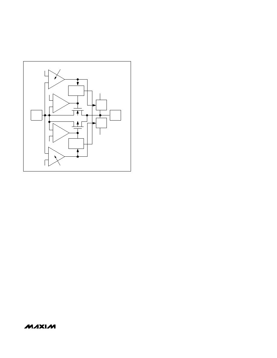
input voltage sensors. The simplified structure is shown
in Figure 1. The parallel N1 and P1 MOSFETs form the
switch element. N3 and P3 are sensor elements to sam-
ple the input voltage and compare it against the power-
supply rails.
During normal operation of a conducting channel, N1
and P1 remain on with a typical 62
on-resistance
between NO_ (or NC_) and COM_. If the input voltage
exceeds either supply rail by about 50mV, the parallel
combination switches (N1, P1) are forced off through
the driver and sensing circuitry. At the same time, the
output (COM_) is clamped to the appropriate supply
rail by the clamp circuitry (N2, P2). Two clamp circuits
limit the output voltage to the supply voltages.
Pin Compatibility
These switches have identical pinouts to common non-
fault-protected CMOS switches (DG401, DG403,
DG405). Exercise care in considering them as direct
replacements in existing printed circuit boards, since
only the NO_ and NC_ pins of each switch are fault pro-
tected.
Normal Operation
Two comparators continuously compare the voltage on
the NO_ (or NC_) pin with V+ and V- supply voltages
(Figure 1). When the signal on NO_ (or NC_) is between
V+ and V-, the switch behaves normally, with FETs N1
and P1 turning on and off in response to NO_ (or NC_)
signals.
For any voltage between the supply rails, the switch is
bidirectional; therefore, COM_ and NO_ (or NC_) are
interchangeable. Only NO_ and NC_ can be exposed
to overvoltages beyond the supply range and within the
specified breakdown limits of the device.
Fault Condition
The MAX4631/MAX4632/MAX4633 protect devices
connected to their outputs (COM_) through their unique
fault-protection circuitry. When the input voltage is
raised 50mV above either supply rail, the internal sense
and comparator circuitry (N3 and N-channel driver or
P3 and P-channel driver) disconnect the output (COM_)
from the input (Figure 1).
If the switch driven above the supply rail has an on
state, the clamp circuitry (N2 or P2) connects the out-
put to the appropriate supply rail. Table 1 summarizes
the switches’ operation under normal and fault conditions.
-15V
+15V
P-CHANNEL
DRIVER
N-CHANNEL
DRIVER
+15V
N3
P3
INPUT
NC_
or
NO_
N1
CLAMP
OUTPUT COM_
CLAMP
+V (+15V)
-V (-15V)
N2
P2
P1
COMPARATOR
SENSE
SWITCH
SENSE
SWITCH
Figure 1. Simplified Internal Structure
相关PDF资料 |
PDF描述 |
|---|---|
| MAX4634EUB | IC MULTIPLEXER 4X1 10UMAX |
| MAX4636EUB | IC SWITCH DUAL SPDT 10UMAX |
| MAX4638EUE+T | IC MULTIPLEXER 8X1 16TSSOP |
| MAX4643EUA | IC SWITCH DUAL SPST 8UMAX |
| MAX4644EUT-T | IC SWITCH SPDT SOT23-6 |
相关代理商/技术参数 |
参数描述 |
|---|---|
| MAX4634ETB | 制造商:Maxim Integrated Products 功能描述:FAST, LOW-VOLTAGE, 4 OHM, 4-CHANNEL CMOS ANALOG MULTIPLEXER - Rail/Tube |
| MAX4634ETB+ | 制造商:Maxim Integrated Products 功能描述:ANLG MUX SGL 4:1 5.5V 10TQFN - Rail/Tube |
| MAX4634ETB+T | 功能描述:多路器开关 IC 4Ohm 4Ch CMOS Analog MUX RoHS:否 制造商:Texas Instruments 通道数量:1 开关数量:4 开启电阻(最大值):7 Ohms 开启时间(最大值): 关闭时间(最大值): 传播延迟时间:0.25 ns 工作电源电压:2.3 V to 3.6 V 工作电源电流: 最大工作温度:+ 85 C 安装风格:SMD/SMT 封装 / 箱体:UQFN-16 |
| MAX4634ETBT | 制造商:Maxim Integrated Products 功能描述: |
| MAX4634ETB-T | 制造商:Rochester Electronics LLC 功能描述: 制造商:Maxim Integrated Products 功能描述: |
发布紧急采购,3分钟左右您将得到回复。